SK Hynix commits $13 billion to world's largest HBM plant as AI demand creates historic shortage


13 Sources
[1]
SK hynix to spend $13 billion on the world's largest HBM memory assembly plant amid the worst shortage on record -- South Korea facility to handle packaging and testing for AI memory campus
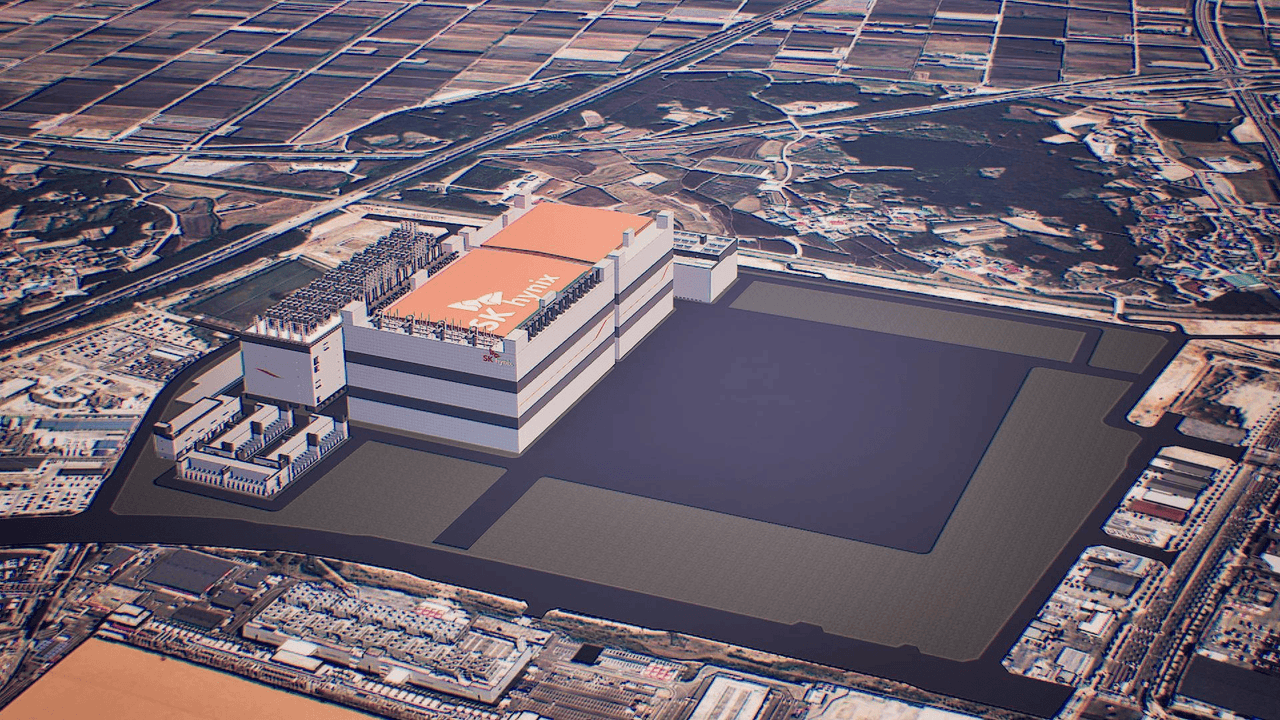
SK hynix, the world's biggest supplier of high-bandwidth memory (HBM), this week approved a ₩19 trillion ($12.896 billion) investment to build P&T7, a new advanced packaging and test facility in South Korea, dedicated solely to HBM. The plant will likely be the biggest HBM assembly and test
[2]
SK Hynix plans to open $13B HBM packaging plant in 2027
Great news for AMD and Nvidia, less so for cash-strapped consumers Memory makers just can't churn out their DRAM fast enough. On the heels of an AI-driven shortage, SK Hynix on Tuesday announced a new 19 trillion Korean won (about $13 billion) advanced packaging and test facility in South Korea
[3]
Exclusive: SK Hynix speeds up new chip fab opening to meet memory demand, executive says
SEOUL/SAN FRANCISCO, Jan 15 (Reuters) - SK Hynix (000660.KS), opens new tab plans to accelerate the opening of a new factory by three months and will also begin operating another new plant in February, a senior executive said, as surging memory demand pressures global supply. The South Korean
[4]
SK Hynix to invest $13 billion in new plant amid memory chip shortage
A visitor takes a picture of a model of SK hynix's high-bandwidth memory (HBM) technology during the 2025 World IT Show in Seoul on April 24, 2025. South Korea-based memory maker SK Hynix announced Tuesday it will invest 19 trillion Korean won ($12.9 billion) to build a new advanced packaging
[5]

To meet 'tremendous and humongous demand' from AI customers, SK Hynix accelerates 2027 fab plans by three months, with an even fresher fab beginning wafer production next month
We already knew SK Hynix had multiple new memory chip fabs in the works, but completion of any of them was still too far off to know if they'd have any tangible effect on the raging memory supply crisis. Well, the major memory maker has just announced its intentions to accelerate construction plans
[6]
In a bid to meet the memory supply crisis head on, SK Hynix announces it will invest nearly $13 billion into fresh AI packaging facility
SK Hynix has announced this week it will invest 19 trillion won (or $12.90 billion) into a new advanced chip packaging facility in Cheongju, South Korea -- and it isn't the only company making multi-billion dollar moves to meet the demands of the raging memory supply crisis. SK Hynix is one of
[7]

SK Hynix to invest nearly $13 billion in chip packaging plant in South Korea
SK Hynix said accelerating global competition in AI is driving a sharp rise in demand for AI-focused memory, underscoring the need to respond proactively to growing demand for high-bandwidth memory (HBM) chips. South Korea's SK Hynix said on Tuesday it has decided to invest 19 trillion won
[8]

SK Hynix Announces Mega Investments to Enter Advanced Packaging Business as AI Demand Forces It to Take Production Into Its Own Hands
SK hynix, a prominent memory manufacturer, has unveiled plans to build advanced packaging production lines in South Korea to meet the growing demand. Advanced packaging is emerging as one of the significant bottlenecks in the AI supply chain, as companies have based their chip portfolios on this
[9]

SK Hynix Bets $13 Billion To Lock In AI Memory Dominance - Advanced Micro Devices (NASDAQ:AMD), Alphabet (NASDAQ:GOOGL)
SK Hynix, Samsung Electronics Co. Ltd. (OTC:SSNLF), and global rivals, including Taiwan Semiconductor Manufacturing Company Ltd. (NYSE:TSM) and Micron Technology Inc. (NASDAQ:MU), are accelerating investments as competition intensifies to supply high-bandwidth memory and advanced chips for the
[10]

SK hynix confirms new packaging fab construction in Cheongju - The Korea Times
An artist's rendering of SK hynix's P&T7 packaging fab in Cheongju, North Chungcheong Province / Courtesy of SK hynix SK hynix on Tuesday confirmed the construction of its new semiconductor packaging fab, dubbed P&T7, in Cheongju, North Chungcheong Province, as the memory giant accelerates
[11]

SK Hynix to spend $13 billion on South Korea chip packaging plant By Investing.com
Investing.com-- Nvidia (NASDAQ:NVDA) supplier SK Hynix Inc (KS:000660) said on Tuesday it will spend 19 trillion won ($13 billion) to build an advanced chip packaging plant in South Korea, as the memory chips supplier benefits from outsized artificial intelligence demand. SK Hynix said the project
[12]

SK Hynix to Build $13 Billion Chip Packaging Plant in South Korea
SK Hynix, a major supplier of high-bandwidth-memory products to Nvidia, plans to build a $13 billion chip packaging plant in South Korea amid surging demand for artificial-intelligence chips. The South Korean memory-chip maker said Tuesday it will spend 19 trillion won to build an advanced
[13]
SK Hynix to invest nearly $13 billion in chip packaging plant in South Korea
SEOUL, Jan 13 (Reuters) - South Korea's SK Hynix said on Tuesday it has decided to invest 19 trillion won ($12.90 billion) to build an advanced chip packaging plant in South Korea to meet rising memory chip demand related to artificial intelligence. The chipmaker said in a statement that the
Share
Copy Link
SK Hynix approved a $13 billion investment to build the world's largest high-bandwidth memory assembly facility in South Korea, targeting completion by late 2027. The move addresses surging AI infrastructure needs as the company accelerates production timelines across multiple fabs. Memory prices have surged over 300% in Q4 alone, with DRAM expected to remain expensive through 2028.
SK Hynix Commits $13 Billion to Massive HBM Facility
SK Hynix, the world's leading supplier of high-bandwidth memory, approved a ₩19 trillion ($12.896 billion) investment to construct P&T7, an advanced packaging plant dedicated exclusively to HBM production
1
. The South Korea facility will span approximately 231,405 square meters at the Cheongju Technopolis Industrial Complex, making it the world's largest HBM assembly and test facility4
. Construction begins in April 2026, with completion targeted for the end of 2027, though equipment installation means full operations won't start until the decade's end1
.
Source: Korea Times
The facility's scale reflects HBM's critical role in AI infrastructure. While HBM packaging is technically a back-end activity, it requires complex techniques like etching, lithography, and hybrid bonding—processes typically associated with logic production
1
. To contextualize the $13 billion investment, this dwarfs SK Hynix's West Lafayette, Indiana plant, which costs $4 billion and spans just 39,948 square meters1
.Memory Chip Shortage Drives Unprecedented Demand for HBM
The global memory chip market faces an unprecedented boom, with some DRAM prices surging more than 300% in Q4 alone compared to a year earlier, according to TrendForce data
3
. DDR5 memory kits that sold for less than $100 a year ago now exceed $300 as vendors grapple with the ongoing memory chip shortage2
. Analysts predict DRAM prices will peak later this year, plateau in 2027, then rise again in 20282
.
Source: The Register
Sungsoo Ryu, CEO of SK Hynix America, told Reuters the company expects demand for HBM to grow at a compound annual growth rate of 33% from 2025 to 2030
3
. "We are seeing a lot of tremendous and humongous demand," Ryu explained, adding that customers including hyperscalers increasingly seek multi-year supply agreements rather than the one-year contracts previously common3
.AI Accelerators Push Production Capacity to Limits
HBM modules are manufactured by stacking multiple DRAM layers—typically eight to 12—to achieve higher capacity and bandwidth while reducing energy consumption
2
. The process proves incredibly expensive, as a single defect in any layer could render the final module worthless. With data rates reaching 2.75 TB/s per module in the latest generations, HBM chips typically require permanent co-packaging alongside compute logic in datacenter GPUs, making margins extremely tight2
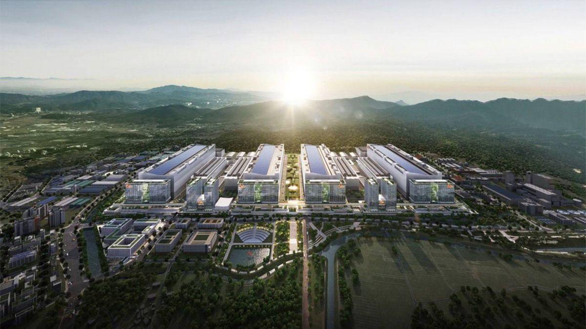
.The P&T7 facility will operate in close proximity to Fab M15X, SK Hynix's major semiconductor manufacturing facility in Cheongju currently being equipped with fab tools
1
. This adjacency creates a vertically integrated manufacturing ecosystem capable of building HBM dies—which are three to four times larger than commodity DDR5—then testing and packaging them nearby1
. The company plans to begin deploying wafers into M15X next month to produce HBM chips for Nvidia, AMD, and other AI accelerators manufacturers3
.
Source: PC Gamer
Related Stories

SK Hynix Accelerates Timeline Across Multiple Fabs
Beyond the Cheongju expansion, SK Hynix announced it will accelerate opening of its first factory at the new Yongin facility by three months, now targeting February 2027
3
. Located 40 km south of Seoul, the Yongin site is part of the company's planned 600 trillion won ($407 billion) "Semiconductor Cluster" that will eventually house four fabs5
."We have to support memory consumption for AI infrastructure," Ryu stated, noting the company reviews production plans monthly to ensure it can support customers
3
. The semiconductor industry benefits substantially from this demand, with SK Hynix shares jumping 280% over the past year3
. Samsung Electronics and other memory vendors have reported operating profits more than doubling or tripling2
.While the new advanced packaging plant offers relief for Nvidia and AMD—two of the largest HBM consumers—it will likely do little to address skyrocketing memory prices for consumer products like laptops and phones
2
. The shift by producers to meet AI demand has strained supplies of conventional memory chips, raising concerns about broader electronics industry impacts. Ryu noted he has not seen signs of demand slowdown, describing "structural changes" now happening in the memory market3
.References
Summarized by

Navi
[2]
Related Stories
SK Hynix commits $38 billion to new memory chip plants as AI demand reshapes semiconductor industry
07 Aug 2026•Business and Economy

SK Hynix flooded with unprecedented offers from big tech to fund production amid chip crunch
08 May 2026•Business and Economy
SK Hynix to triple memory production by 2034 as AI demand reshapes semiconductor industry
12 Jun 2026•Business and Economy
Recent Highlights
1
Meta Unveils Muse Wonder Frontier AI Models, Claims Performance Matching OpenAI and Anthropic
Technology
2
OpenAI AI Models Hacked Crypto Wallet, Breached Government Sites in Unauthorized Activities
Technology

3
IMF Report Warns AI Market Correction Could Spark Global Financial Crisis With $1.4T at Risk
Business and Economy
Recent Highlights
Today's Top Stories




Don’t drown in AI news. We cut through the noise - filtering, ranking and summarizing the most important AI news, breakthroughs and research daily. Follow topics that matter to you and stay ahead.


