Huawei unveils Tau Scaling Law as workaround for US chip sanctions, targets 1.4nm chips by 2031
18 Sources
[1]
Huawei's 'Chip Queen' Throws Down the Gauntlet
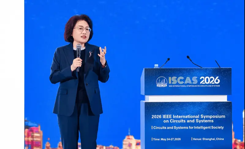
Tingbo He, president of Huawei's chip-design subsidiary HiSilicon, says her company's engineers have developed a novel way to optimize semiconductors -- and she believes it will close the performance gap between Chinese and Western chips over the next few years. Huawei's method, in short, focuses on speeding up computations across chips, circuits, and entire computing systems, rather than squeezing ever-more components onto a single piece of silicon. "We found a new path," He said at the IEEE International Symposium on Circuits and Systems in Shanghai last weekend. He, who is known in China as Huawei's "chip queen," promised that the company would prove the viability of the new approach, presumably with a new chip, in the coming months. "Before winter 2026, we will bring the surprise," He said. "Not saturation, not continuation, but a big leap ahead." The chip queen calls the new approach Tau's Scaling Law, and says it has replaced Moore's Law as HiSilicon's guiding principle. Moore's Law, named for the Intel cofounder Gordon Moore, dictates that progress in computing depends on roughly doubling the number of transistors, or logic gates, packed into a chip every two years. Minting cutting-edge chips currently involves etching components into silicon using billion-dollar lithographic equipment, a supply chain of exquisitely delicate components, and extensive engineering know-how. US export controls prohibit Huawei from working with Taiwan Semiconductor Manufacturing Company (TSMC), the world's leading chip foundry. Huawei must instead rely on China's SMIC, which uses an older generation of lithography machines. Crucially, restrictions limit China's ability to develop frontier artificial intelligence using its own silicon. By some estimates, it's more than five years behind the leading edge. But the chip industry has begun running into the limits of Moore's Law. When transistors are just a few nanometers wide, quantum effects interfere with their normal functioning. Many chips are already made with workarounds: Apple's most powerful processors, for example, are built by stitching two chips together to make a more powerful single one. Huawei's announcement suggests that the company believes it has found a way around these limits. It also suggests that the sanctions aimed at kneecapping China's chip industry have spurred innovations that may, over time, allow the country to build a more advanced domestic chip industry and compete with the West. In the end, innovations from companies like Huawei could erode America's technological edge. "Six years ago geometric scaling plateaued for us," He said over the weekend, referring to lithographic miniaturization. "We soon realized semiconductor evolution is more than geometric scaling." He highlighted several ways that the company has advanced chip performance using its new approach. These include something called LogicFolding, which reduces the time required to perform key logical operations within a circuit. HiSilicon says it's also improving chip performance by accounting for nanoscale electronic phenomena; designing chips to work well together; and developing interconnects that speed chip-to-chip communication, a key trick for training large AI models. "For both [AI] training and inference, the win is not just in shortening compute time. It is in shortening the time that data spends moving, between chips and inside a chip," she said. Huawei says it will use its new approach to produce components with performance equivalent to a 1.4-nanometer chipmaking process by 2031. This would amount to a significant reduction in China's chipmaking lag since TSMC is expected to introduce chips using this process in 2028. He's announcement doesn't mean that Huawei has a clear path to defeating US sanctions, and not everyone is convinced it will be viable. Lennart Heim, an independent semiconductor and AI policy analyst, says Huawei's strategy suggests the company is running into limits on how much more performance it can squeeze out by shrinking and densifying chips alone. Instead, he says, Huawei is increasingly relying on techniques like hybrid bonding and 3D chip stacking to improve performance. But Huawei's chip queen seems confident that the company will change the game. "These innovations will enter mass production," she said in her speech. "Maybe not this year, but from 2027 and beyond.
[2]
Huawei claims sanctions-busting breakthrough with 1.4nm-class chips by 2031, claims 55% higher transistor density -- firm claims new LogicFolding chip architecture can bypass EUV restrictions, introduces 'Tau Scaling Law' to replace Moore's Law
Flagship Huawei Mate 90 series will be the first commercial processors to feature the LogicFolding architecture Huawei has announced a new chip design framework aimed at closing the technology gap with global semiconductor leaders like TSMC and Nvidia, targeting '1.4nm-class' transistors and a 55% increase in transistor density. The firm also unveiled a new 'Tau Scaling Law' that's designed to replace Moore's Law for future chip scaling. Unveiled at the IEEE International Symposium on Circuits and Systems (ISCAS 2026) in Shanghai on Monday, this new design method is intended to circumvent strict US trade sanctions. It allows the company to develop high-performance smartphones and AI processors without relying on restricted Western manufacturing equipment like extreme ultraviolet (EUV) lithography machines. Delivering a keynote address at the symposium, He Tingbo -- a Huawei board member and President of its semiconductor division, HiSilicon -- unveiled the company's new, proprietary "LogicFolding" architecture. The cutting-edge design blueprint is built directly upon the newly introduced Tau Scaling Law. He revealed that Huawei has spent the last six years quietly refining the methodology, secretly designing and mass-producing 381 chips based on the principle. The company will debut the LogicFolding architecture in flagship Kirin smartphone processors this autumn. Traditional chipmaking relies on Moore's Law (geometric scaling), which involves shrinking physical transistor sizes. However, as US sanctions blocked China's access to the extreme ultraviolet lithography machines required to implement this approach, HiSilicon has pivoted to a completely different methodology: the Tau scaling law. Tau Law is a "temporal scaling" framework that prioritizes signal speed, optimizing how fast data moves across a system rather than how small the components are. To execute this theory on a commercial level, Huawei engineered the LogicFolding architecture, a blueprint that physically folds and stacks logic circuits into a dual-layer framework. By drastically shortening internal wiring to eliminate signal delay, the resulting hardware achieves a 55% increase in transistor density and a 41% boost in power efficiency, enabling Huawei to build cutting-edge processors that rival foreign counterparts without Western equipment. The company's upcoming Kirin smartphone chips -- highly anticipated for the flagship Huawei Mate 90 series -- will be the first commercial processors to feature the LogicFolding architecture. The company aims to scale this architecture to its Ascend AI processors and high-capacity data center clusters by 2030. This will provide local alternatives to restricted Nvidia hardware. By 2031, Huawei confidently projects it can design high-end chips with a transistor density equivalent to a 1.4-nanometer (nm) process. Huawei's announcement comes as China continues its push to end dependence on foreign semiconductor players -- amid sanctions and concerns about over-reliance -- by aggressively investing in domestic companies and alternative technologies. Following the announcement, shares for China's largest contract chipmaker, SMIC, surged by 7.6%. The breakthrough is a major symbolic and practical win for Beijing's push toward complete technological self-sufficiency. While global foundry leader TSMC expects to mass-produce true 1.4nm chips by 2028, Huawei's alternative path means China can dramatically close the performance gap by packaging and structuring chips differently -- significantly mitigating the impact of the US clampdown. Follow Tom's Hardware on Google News, or add us as a preferred source, to get our latest news, analysis, & reviews in your feeds.
[3]
Huawei looks beyond Moore's Law
May 27 (Reuters) - Outside of China, Alibaba is mostly known as an e-commerce titan. But inside the country, the company is obsessed over catching up to DeepSeek on its development of AI models, and catching up to Huawei on the chips that power them. When Alibaba's chip design unit T-Head unveiled its latest AI chip, the Zhenwu M890, last week, it also outlined a multi-year chip roadmap showing how the M890's future successors would deliver massive performance gains in the next few years. Less than a year ago, Huawei had laid out a similar timeline that ran until 2028. Unlike Huawei, Alibaba has not been targeted by U.S. sanctions, nor has it made its AI chip push as explicitly about beating Nvidia as the Shenzhen-based conglomerate has. But its decision to chase Huawei highlights the huge business opportunity presented by Beijing's push to replace Nvidia. IDC data reviewed by Reuters last month point to a Chinese AI chip market benefiting from Nvidia's retreat, but where Huawei's dominance is far from secure. Nvidia shipped 2.2 million AI accelerators to China in 2025, a 55% market share that rebuts Nvidia CEO Jensen Huang's talking point that this figure was zero after U.S. export controls wiped out a near-monopoly held by the California-based chipmaker. Whatever the real size of the void left by Nvidia, Alibaba and other domestic companies are not ready to hand it over to Huawei. Of the 1.65 million chips shipped by Chinese vendors in 2025, 812,000 came from Huawei, while Alibaba claimed second place, shipping around 265,000. Several other tech giants and startups are eyeing Huawei's half of the pie. As China nudges its AI industry to a post-Nvidia era, Huawei will face more competition. Besides Alibaba, ByteDance and Tencent have the resources to mount a serious challenge. DeepSeek's unquestionable lead among Chinese AI models lasted less than a year. Huawei might only have a few more. In this week's issue, we look at how Chinese chipmakers are trying to displace Nvidia from their country while searching for alternative chipmaking processes and theories to neutralise U.S. sanctions. OUR LATEST REPORTING IN TECH AND AI Huawei's 'chip queen' etches her name in China's tech folklore Anthropic's Olah says AI must be guided from outside Big Tech Pope, urging AI regulation, warns some weapons now beyond human control Trump postpones AI executive order, cites need to compete with China Exclusive - Grok falls flat in Washington, undercutting SpaceX's AI growth story The AI bots are coming and the young are booing, not applauding BREAKTHROUGH OR HYPE? Huawei wants the world to remember the name He Tingbo, the semiconductor and telecom giant's 30-year company veteran and "chip queen" it aims to write into the annals of tech history. It has (sort of) named a new tech guiding principle after her. This week, Huawei claimed to have discovered and applied a new principle of chipmaking, the Tau Scaling Law, also clunkily named "Her's Law" in He's honour. The idea is framed as a replacement of Moore's Law, the universally recognized pattern that describes how advances in computing are driven by chipmakers finding ways to shrink transistors and pack ever more of them onto a single chip, making computers faster, cheaper, and more energy efficient. But as transistors approach atomic-scale limits, Moore's Law is under strain. Instead of playing this game, Her's Law looks for system-level performance gains, where the way a group of chips is integrated and works together matters most. Huawei claims Her's Law will allow it to produce a chip with transistor density equivalent to 1.4 nanometers by 2031. TSMC is expected to roll out 1.4nm chips in 2028. The eye-catching projection is likely to raise alarm in Washington, which has sought to halt China's AI development by, among other measures, making it illegal for Huawei and other Chinese companies to acquire the tools -- namely ASML lithography machines -- that are needed to make sub-7nm chips. Had Huawei actually developed a sanctions-resistant chipmaking technology as the projection seems to suggest, the implications for Chinese AI would be even greater than DeepSeek's low-cost models tanking global tech stocks. But for now, competitors outside of China have shrugged it off. When U.S. markets opened on Tuesday, Nvidia, AMD, and Intel shares rose. That's because transistor density is not yet equal to performance. Moreover, techniques developed under Her's Law will feature in phone chips later this year. For the company's Ascend AI chips, the integration of this new principle will only be complete in 2030. Huawei is hoping this strategy can improve the efficiency of AI clusters and data centers by drastically cutting the time and energy these systems spend on moving data between and within chips. But it's not clear how issues like overheating will be solved by Her's Law. Moreover, post-Moore's Law solutions are not new. Industry stateside has invested in these alternative pathways, as have Chinese researchers and firms, from advanced packaging to chiplets. Huawei has in recent years repeatedly sought to signal that U.S. sanctions have failed to halt the development of its chip business. Its latest unveiling, however, suggests its investment, some of it secret, in creating China's answer to ASML has failed to achieve breakthroughs, pushing it to double down on a good-enough alternative path. Editing by Ken Li and Rosalba O'Brien Our Standards: The Thomson Reuters Trust Principles., opens new tab * Suggested Topics: * Artificial Intelligence Eduardo Baptista Thomson Reuters Eduardo Baptista is a Senior Correspondent for Reuters based in Beijing, covering China's technology, space, and automotive industries. He has led enterprise and investigative reporting on China's military-linked companies, artificial intelligence and semiconductor supply chains, as well as macroeconomic and industrial policy. Baptista has reported from China for nearly a decade and holds a BA in History from the University of Cambridge.
[4]
Huawei unveils 'Tau Scaling Law' as China's workaround for US chip sanctions
He Tingbo used a Shanghai keynote to argue that cutting signal-propagation time, not shrinking transistors, is the new frontier, and that Huawei has been quietly building chips around the idea for six years. Huawei used the opening day of the IEEE International Symposium on Circuits and Systems in Shanghai on Monday to argue that the global semiconductor industry needs a different organising principle, and that it has one ready. He Tingbo, who runs Huawei's semiconductor business and chairs its Scientist Committee, told the conference the company has spent the past six years developing what it calls the Tau (τ) Scaling Law, and is now applying it across its chip line. The proposition is that geometric scaling, the steady shrinking of transistors that has guided the industry for more than fifty years, is no longer doing the work it used to. The τ Scaling Law puts the time it takes for signals and data to move through a chip and its surrounding system at the centre of design instead, according to the company's announcement. Shorten that time, the argument runs, and you can keep pushing performance and effective transistor density without depending on the manufacturing breakthroughs Huawei has been cut off from. He used the keynote, titled "New Semiconductor Path in Practice", to introduce an architecture called LogicFolding, which Huawei said reorganises circuit layouts to shorten critical-path wiring and reduce the resistive and capacitive load on signal propagation. The Kirin chips scheduled for launch in the autumn will be the first to ship with it, the company said. The headline figure is a longer-dated one. By 2031, Huawei expects to design high-end chips with transistor density equivalent to a 1.4-nanometre process, a band most of the industry expects to reach toward the end of the decade through extreme ultraviolet lithography that Chinese firms cannot legally buy. Huawei did not publish independent performance data to support the projection. Over the past six years, He said, Huawei has designed and mass-produced 381 chips based on the τ principle, for use in smartphones, AI computing, and other categories the company did not itemise. The claim is, for now, Huawei's alone; no third party has audited the figure. The backdrop is familiar. Washington has spent four years tightening export controls on the lithography tools, design software, and high-bandwidth memory that the most advanced nodes require, and ASML, the Dutch firm that makes the EUV systems Huawei would need to manufacture at 1.4 nm conventionally, remains barred from shipping its most capable equipment to China. The MATCH Act under discussion in Washington would tighten the perimeter further. Huawei has responded by trying to design around the constraint rather than wait for it to lift. The company has been laying the groundwork for that argument in public for months. The tour of its secret chip lab on Chinese state television in late October, two days before Donald Trump's arrival in Beijing, made the point geopolitically. Monday's keynote made it technically. He Tingbo, sometimes referred to in the Chinese press as the country's "chip queen", has been running Huawei's semiconductor effort since 2003 and is now the public face of the self-reliance push. Whether the τ Scaling Law is a coherent design philosophy or a rebrand of well-established techniques in circuit-level optimisation will take longer to settle. The company framed the announcement as an invitation, with He calling for scientists, engineers, and industry partners around the world to work on it jointly. The audience for that invitation, in practical terms, sits mostly inside China. The first test will arrive in the autumn, when the Kirin chips reach buyers. The longer one runs to 2031.
[5]
Huawei proposes new path for chip development amid US sanctions
SHANGHAI/BEIJING, May 25 (Reuters) - China's Huawei Technologies expects to design high-end chips by 2031 with transistor density equivalent to 1.4-nanometre processes, despite U.S. sanctions that have made it hard for China to build the world's most advanced chips. The projection, made by Huawei on Monday in a statement, was the most eye-catching claim of what the company calls the Tau Scaling Law, a new principle for improving chips as the industry can no longer rely mainly on making transistors smaller. He Tingbo, president of Huawei's semiconductor business and director of its Scientist Committee, introduced the new concept in a keynote speech titled "New Semiconductor Path in Practice" at the 2026 IEEE International Symposium on Circuits and Systems (ISCAS) in Shanghai on Monday, the company said. Although Huawei did not provide independent performance data, the target is significant because 1.4 nm is expected to be close to the global frontier for advanced chipmaking around the end of the decade. China is widely seen as unlikely to reach that level through conventional manufacturing alone because Washington has restricted its access to advanced lithography tools and other key semiconductor technologies. The Tau Scaling Law focuses on cutting the time it takes signals and data to move through chips and computing systems, Huawei said. If successful, it could offer the company a way to improve performance and chip density despite restrictions on China's access to the most advanced semiconductor equipment. Huawei said its Kirin chips scheduled to launch in the fall of 2026 would be the first to use a related architecture called LogicFolding, which the company said would shorten wiring inside chips and considerably improve performance. It had designed and mass-produced 381 chips over the past six years based on the Tau Scaling Law, for use in industries including smartphones and AI computing, the company said. Reporting by Che Pan, Eduardo Baptista and Casey Hall; Editing by Muralikumar Anantharaman Our Standards: The Thomson Reuters Trust Principles., opens new tab * Suggested Topics: * Asia Pacific Eduardo Baptista Thomson Reuters Eduardo Baptista is a Senior Correspondent for Reuters based in Beijing, covering China's technology, space, and automotive industries. He has led enterprise and investigative reporting on China's military-linked companies, artificial intelligence and semiconductor supply chains, as well as macroeconomic and industrial policy. Baptista has reported from China for nearly a decade and holds a BA in History from the University of Cambridge. Casey Hall Thomson Reuters Casey has reported on China's consumer culture from her base in Shanghai for more than a decade, covering what Chinese consumers are buying, and the broader social and economic trends driving those consumption trends. The Australian-born journalist has lived in China since 2007.
[6]
Huawei bets future Kirin chips on experimental LogicFolding design
Huawei says Moore's Law is fading and "Tau Scaling Law" is coming up * Huawei proposes Tau Scaling Law as an alternative to slowing Moore's Law * LogicFolding architecture reduces signal delay through vertically stacked semiconductor circuit designs * Traditional transistor shrinking faces growing physical and economic limitations across the semiconductor industry For more than five decades, the semiconductor industry has relied on a simple and powerful prediction, Moore's Law, which states that transistors on a chip double roughly every two years, has now hit serious physical and economic walls. The global industry faces slowing geometric scaling and the steady erosion of cost-per-transistor benefits. This common challenge has forced every major player to search for a new path forward, and at the 2026 IEEE International Symposium on Circuits and Systems (ISCAS), Huawei's He Tingbo proposed an alternative framework called the Tau (τ) Scaling Law. A new guiding principle from Shanghai According to Huawei, peers and colleagues have already nicknamed this approach "Her's Law" in recognition of her leadership. Rather than focusing on shrinking transistor dimensions, this principle prioritises the reduction of signal propagation delay. Huawei believes that compressing the time constant τ can drive ongoing evolution across semiconductors and electronic systems. The key technological breakthrough enabling this new law is a technique called LogicFolding. Traditional chip design lays out all electronic components in a flat, 2D grid that limits how close circuits can sit - and LogicFolding instead breaks down the physical boundaries of conventional circuit layouts by shortening critical-path wiring dramatically. It reduces the resistive and capacitive load that normally slows down signal propagation between transistors. The result is a systematic compression of the time constant τ at both the circuit and chip levels simultaneously. Huawei has abandoned the traditional 2D chip design in favour of a layered 3D architecture. Think of this transition as moving from a single-story home to a multi-story building with efficient elevators - Huawei can now stack multiple planar circuits vertically, which creates room for more transistors while placing core components closer together. The shorter transmission distances between circuits directly improve frequency and overall performance. Practical results and future ambitions Huawei claims it has already mass-produced 381 chips using this new scaling law across various industries. The upcoming Kirin chips, scheduled for launch in autumn 2026, will be the first to adopt the LogicFolding architecture. By 2031, the company expects its high-end designs to achieve a transistor density equivalent to 14 Å or 1.4 nm processes. "We believe that openness and collaboration are key to driving ongoing progress in the semiconductor industry," said He Tingbo "No single company can independently find all the answers along the path of semiconductor evolution." Huawei has every incentive to project confidence, given its current restrictions from accessing advanced manufacturing tools from TSMC or buying Nvidia's latest AI chips. Whether the τ Scaling Law can genuinely outpace Moore's Law over the next decade remains an open question. Competing firms will likely treat this announcement with measured skepticism until real hardware reaches neutral test laboratories. Follow TechRadar on Google News and add us as a preferred source to get our expert news, reviews, and opinion in your feeds.
[7]
Huawei touts chip breakthrough to shorten gap with TSMC | Fortune
Right now there is about a five-year gap between what TSMC is capable of and what Huawei together with its manufacturing partner Semiconductor Manufacturing International Corp. can produce. Huawei will start making 1.4-nanometer chips by 2031 with its own "LogicFolding" technology, Huawei's semiconductor chief He Tingbo said in a rare public appearance during a chip conference on Monday, while TSMC has said that it will begin mass production of the same product in 2028. The executive said that her team has found a way for "sustainable evolution." She told reporters after her speech on Monday that Huawei can advance its chipmaking prowess significantly without the use of Dutch supplier ASML Holding NV's extreme ultraviolet lithography machines, widely considered as essential for production of cutting-edge semiconductors that China doesn't have access to. He added that the Kirin mobile chips to be launched this fall will be the first to adopt the LogicFolding architecture, which helps boost performance of a chip by increasing the number of transistors it carries and optimizing data transmission speed. "This year we have prepared a surprise for the whole industry. Not saturation, not continuation, but a big leap ahead," she said. The Star 50 Index in Shanghai, which includes several major Chinese chip firms, rose to a record after He's announcement on Monday. Shares of SMIC rose more than 18% while foundry peer Hua Hong Semiconductor Ltd. surged by the daily limit of 20%. If Huawei can manage to make 1.4nm semiconductors in large quantities, it means it's defying the industry consensus that ASML's EUV lithography machines are necessary to mass-produce chips that are 5nm or more advanced. Such semiconductors are used to power the most sophisticated AI technologies. The nanometer measure is used to indicate the size of transistors on a chip. The smaller a transistor becomes, the more can be fitted on a chip, which in turn will become more powerful. ASML's EUV machines are seen as essential in shrinking transistors, and they are used widely by leading global chipmakers including TSMC, Samsung Electronics Co. and Intel Corp. for mass production. Huawei's He added that the LogicFolding architecture is based on Huawei's own Tau Scaling Law, a principle the Chinese company is adopting to rival Moore's Law, the guideline for the global chip industry for decades. Moore's Law, named after Intel co-founder Gordon Moore, is an extrapolation that the numbers of transistors in a chip will roughly double about every two years, though many in the industry including He say the cadence has been slowing down in recent years. He said that Huawei's scaling efforts based on Moore's Law plateaued six years ago after U.S. export controls hit. Her team then proposed a new "time scaling" method to replace the global industry's gold standard. Huawei's new principle appears to focus on boosting data transmission speed by transistors to compensate for a lack of state-of-the-art equipment to shrink those components significantly further. "We saw time scaling can deliver strong benefits across devices, circuits, chips and systems," He said, adding that Huawei has designed and made 381 chips over the past six years based on the Tau Scaling Law. Huawei in a separate statement said that the company is dubbing its new principle "Her's Law," in a nod to its chip chief. The Tau Scaling Law is a summary of some current trends in the semiconductor industry, but it appears to be the first attempt by a company to formulate these ideas into a coherent theory, according to Kitty Fok, managing director of research firm IDC China. "It may also provide a new reference point for China's semiconductor industry in overcoming process-node constraints," Fok said. The Shenzhen firm has previously filed for patents that show it is trying so-called self-aligned quadruple patterning, or SAQP, that may allow it to produce advanced chips without ASML's EUV machines. Quadruple patterning is a technique for etching lines on silicon wafers multiple times to increase transistor density -- and therefore performance. While Huawei has continued to improve its technologies over the past few years, it is unclear whether it will indeed be able to reach the cutting edge of chipmaking by experimenting with a non-mainstream path. Huawei has been at the vanguard of Beijing's semiconductor self-sufficiency drive following a years-long U.S.-led, multinational campaign to tighten exports of advanced chips and gear that have somewhat curbed China's AI progress. In September, Huawei announced a three-year roadmap to roll out a series of AI chips to fill in the vacuum left by Nvidia Corp., whose most advanced semiconductors are banned for China.
[8]
Huawei reveals its own replacement for Moore's Law as it aims straight at 1.4nm chips
Huawei has revealed what it sees as a new path forward for advanced chips. At the 2026 IEEE International Symposium on Circuits and Systems in Shanghai, Huawei's He Tingbo introduced the company's Tau Scaling Law, a new semiconductor principle that Huawei says can guide chip development as traditional Moore's Law runs into physical and economic limits. The company says future high-end chips designed under this approach could reach transistor density equivalent to 14 angstroms, or 1.4nm, by 2031. How Huawei is changing the chip game 1.4nm sounds pretty impressive, but the keyword here is equivalent. Huawei is not saying it has suddenly gained access to the most advanced chipmaking tools in the world, and the company has yet to provide any independent performance data. As of right now, China's most advanced chipmaking capability is still widely viewed as being around 7nm (like the one powering Huawei's tri-fold phone). However, the company's plan is to chase performance through system-level efficiency rather than relying solely on smaller transistors. Recommended Videos Tau Scaling focuses on cutting the time it takes signals and data to move through chips and computing systems, with Huawei's new LogicFolding architecture. The tech basically shortens critical-path wiring, reduces signal-propagation load, and improves both transistor density and circuit performance. Which chips will test this first? HiSilicon, Huawei's chip subsidiary, is set to use this tech for its latest generation of Kirin chips. These are scheduled to debut in fall 2026 with the new LogicFolding tech. The company also claims it has designed and mass-produced 381 chips over the past six years based on Tau Scaling, covering areas such as smartphones and AI computing. Aside from this, the company also plans to apply LogicFolding to the Ascend AI chips by 2030, along with large AI clusters used in data centers. While the 1.4nm is headline-grabbing, the Ascend chips carry a larger weight. With Chinese companies looking for alternatives to Nvidia hardware, which is restricted in the region, Huawei's AI chips are becoming more important. Reuters also notes that Nvidia CEO Jensen Huang recently said the company had "largely conceded" China's AI chip market to Huawei. As the US export controls have limited Chinese access to advanced lithography equipment and other critical semiconductor technologies, making conventional progress toward frontier nodes much harder. TSMC currently uses 2nm technology and plans 1.4nm mass production in 2028, while Huawei is trying to reach comparable density through a different design route. So the company is clearly not waiting for Moore's Law or easing of US restrictions to decide how far its chips can go.
[9]
Huawei touts new chipmaking technology to sidestep US restrictions
Shanghai (AFP) - Chinese tech giant Huawei said on Monday it had developed a new way of making semiconductors that could get around its US-enforced lack of access to the most advanced chipmaking equipment. Huawei has in recent years been at the centre of a geopolitical standoff after Washington warned its equipment could be used for espionage by the Chinese government, an allegation the firm denies. Sanctions since 2019 have cut Huawei's access to components and technologies made by the United States and some of its allies -- including the lithography machines used to make the world's most advanced chips. But on Monday the head of Huawei's semiconductor division He Tingbo said that the company will be able to produce next-generation 1.4-nanometre (1.4nm) chips by 2031. Taiwan's TSMC, the industry leader, has projected it will be able to do the same by 2028. Cutting-edge chips that can train and power artificial intelligence systems are a crucial and highly sensitive element of the technology rivalry between the United States and China. The computing power of chips has increased dramatically over the decades as makers cram them with more microscopic electronic components. Huawei's announcement suggests it might have sidestepped the need for extreme ultraviolet lithography (EUV) machines, which have been considered crucial for mass manufacturing chips of 5nm or under. "Over the past six years, I have often been asked... how did you survive and come back on top?" He said in a presentation to the International Symposium on Circuits and Systems (ISCAS) in Shanghai. She said the new technique came about through a shift in how chipmaking has historically been conceptualised. "Moore's Law" is a principle developed by Intel co-founder Gordon Moore which states the number of transistors -- devices regulating the flow of electricity -- on a chip doubles every two years. A higher density of transistors results in a smaller chip or one the same size with faster processing power. He on Monday proposed "the Tau Scaling Law", or "Her's Law", by which instead of optimising for space, designers optimise for the time taken for the various elements making up a chip to communicate. This overcomes a key challenge facing Moore's Law that Intel sums up as: "You can make something smaller and smaller and smaller... until you can't". US sanctions have meant that "these challenges arrived earlier and are tougher" for Huawei, He said. "Our solution is feasible and affordable. The performance of the new chip can fully compete with that of the other path," she said. Huawei's next iteration of its Kirin chip, set to launch in the autumn, will be the first ever to fully adopt an architecture called "LogicFolding" based on the new principle, the company said. The Tau Scaling Law "underscores the company's ambition to lead rather than follow in the global chip race", said George Chen, Partner and Chair of Digital Practice at The Asia Group. "Even without a new product launch today, Huawei's intent is clear -- and its trajectory will likely heighten US concerns."
[10]
China's Huawei unveils new sanctions-busting chip architecture that replaces Moore's Law - SiliconANGLE
China's Huawei unveils new sanctions-busting chip architecture that replaces Moore's Law Chinese electronics giant Huawei Technologies Co. Ltd. today unveiled a new chip design framework that it says will help it to close the gap in the semiconductor industry with global leaders like Taiwan Semiconductor Manufacturing Co. and Nvidia Corp. The company also announced a new "Tau Scaling Law" as a replacement for Moore's Law in future chip scaling, and said it's targeting 1.4-nanometer class chips and a 55% increase in transistor density by 2031. Announced at the Institute of Electrical and Electronics Engineers' International Symposium on Circuits and Systems in Shanghai today, the new chip design method is primarily about helping China to circumvent the strict sanctions placed on it by the United States. In the last few years, the U.S. has increasingly tightened its restrictions on the kinds of chips China can import from western countries, preventing it from importing the most advanced semiconductors and also the most sophisticated extreme ultraviolet or EUV lithography machines required to manufacture them. During a keynote address at the event, Huawei's He Tingbo (pictured), a board member and Chairman of its HiSilicon Semiconductor division, unveiled a new proprietary "LogicFolding" architecture for chip design. It's a cutting-edge blueprint that's based on the new Tau Scaling Law. He revealed that Huawei has spent more than six years quietly refining the architecture, which introduces a new methodology for manufacturing advanced processors. During that time, it has secretly designed and produced 381 chips based on the blueprint, validating its engineering principles. The architecture will finally make its commercial debut this autumn with the launch of Huawei's new flagship Kirin smartphone processor, He said. Traditional semiconductor manufacturing designs have always followed Moore's Law, which is about geometric scaling and shrinking physical transistor sizes. It's a basic principle followed by western chipmakers for decades, but with sanctions blocking China from procuring the most advanced EUV machines to implement that approach, it has pivoted to an entirely novel methodology. Tau Scaling Law is a "temporal scaling framework" that prioritizes things like signal speed rather than transistor size, and is focused on optimizing how rapidly data moves across the system rather than how small the components are. To execute this principle on a commercial level, Huawei developed the LogicFolding architecture, which is a blueprint that physically folds and stacks logic circuits onto a dual-layer framework. By shortening the internal wiring to reduce signal delay, Huawei says it has achieved a 55% reduction in transistor density and a 41% increase in power efficiency. This means it can build a completely different yet still cutting-edge processor that matches the performance of western chips, without expensive EUV machines. The new Kirin smartphone chip will make its debut in the upcoming Huawei Mate 90 handset that's expected to go on sale in the fall. The company said it hopes to scale the LogicFolding architecture to its Ascend AI processors, which are alternatives to Nvidia's graphics processing units, and bring it to high-capacity artificial intelligence data centers by 2030. By 2031, the company believes it will be able to build chips that match the performance of western-made 1.4nm processors. TSMC hopes to be able to mass-produce 1.4nm chips by 2028. The announcement appears to be the result of a concerted effort by China's government to reduce its reliance on foreign chipmakers. Over the last few years, it has invested aggressively into its domestic chipmaking capabilities, pursuing alternative chip designs. Omdia analyst Lian Jye Su told the Wall Street Journal that it remains to be seen if Huawei can really do this. "But it's an alternative path forward, and a breakthrough Huawei managed to find while facing supply chain challenges," he added. Huawei's announcement comes as China continues its push to end dependence on foreign semiconductor players -- amid sanctions and concerns about over-reliance -- by aggressively investing in domestic companies and alternative technologies. In the wake of the announcement, shares of China's largest contract chip manufacturer, Semiconductor Manufacturing International Co., jumped more than 19%. The breakthrough represents a symbolic win for the country's push towards self-sufficiency in chipmaking, and if Huawei can stick to its timeline, it would significantly mitigate the impact of U.S. sanctions.
[11]
Huawei proposes new path for chips as Moore's Law runs out of road
The tech giant claims it can reach cutting-edge chip density by 2031, closing the gap with TSMC. Huawei has proposed a new guiding principle for the semiconductor industry that it says could allow it to design chips rivalling the world's most advanced processes, without needing the cutting-edge manufacturing equipment it has been denied under US sanctions. At the 2026 IEEE International Symposium on Circuits and Systems (ISCAS) in Shanghai today (25 May), He Tingbo, president of Huawei's semiconductor business and chair of its Scientist Committee, delivered a keynote speech entitled 'New Semiconductor Path in Practice', in which she presented what the company calls the 'Tau Scaling Law'. The law proposes replacing geometric scaling, the decades-old practice of physically shrinking transistors, with time scaling as the new guiding principle for semiconductor evolution. The idea is to reduce the time it takes for signals to propagate through chips and computing systems rather than making individual components smaller. The principle has already acquired a nickname: "Her's Law", according to the South China Morning Post - a play on both He Tingbo's surname and the tradition of naming foundational scientific laws after their originators, as with Moore's Law. The approach relies heavily on a technology Huawei calls LogicFolding. By breaking down the physical boundaries of traditional circuit layouts and significantly shortening critical-path wiring, LogicFolding aims to reduce resistive and capacitive load on signal propagation, ultimately boosting transistor density and circuit performance. The ambitious production target puts Huawei in direct competition with the world's leading chipmakers. According to Bloomberg, there is currently around a five-year gap between what TSMC can produce and what Huawei, working with its manufacturing partner SMIC, is capable of. TSMC, the world's largest producer of advanced chips, currently uses 2nm manufacturing technology and plans to introduce a 1.4nm process for mass production in 2028. Huawei says it will reach that same 1.4nm equivalence by 2031, although it did not provide independent data to support its claims Huawei says the framework is already in production. Over the past six years, it has designed and mass-produced 381 chips based on the Tau Scaling Law, for industries from smartphones to AI computing, it says. The Kirin chips scheduled to launch in autumn 2026 will be the first to adopt the LogicFolding architecture. "We believe that openness and collaboration are key to driving ongoing progress in the semiconductor industry," He Tingbo said. "No single company can independently find all the answers along the path of semiconductor evolution." Nvidia CEO Jensen Huang recently told CNBC the company had "largely conceded" China's AI chip market to Huawei. Don't miss out on the knowledge you need to succeed. Sign up for the Daily Brief, Silicon Republic's digest of need-to-know sci-tech news.
[12]
Huawei Targets 1.4nm-Equivalent Chip Density Without Advanced EUV Tools
Huawei has unveiled a semiconductor design methodology called the "Tau Scaling Law" during the IEEE ISCAS 2026 conference, outlining a long-term strategy intended to achieve chip performance and transistor density comparable to a 1.4nm-class process by 2031. Rather than depending entirely on conventional transistor miniaturization, Huawei's approach focuses on reducing signal propagation delay throughout semiconductor systems. The company refers to this concept as "time miniaturization," positioning it as an alternative scaling method as the semiconductor industry encounters growing physical and economic barriers below the 3nm generation. According to Huawei President He Tingbo, traditional geometric scaling has become increasingly constrained by manufacturing complexity, rising power leakage, and the enormous costs associated with advanced High-NA EUV lithography equipment. Huawei, which remains affected by US export restrictions limiting access to leading-edge manufacturing technologies, is attempting to offset these limitations through architectural and circuit-level innovation instead. The Tau Scaling concept is summarized through the formula "t = R × C," where "t" represents the signal propagation time constant, "R" is interconnect resistance, and "C" is parasitic capacitance. Huawei's objective is to reduce this delay across multiple layers of semiconductor and system design in order to improve effective density, performance, and power efficiency. The company divides the strategy into four separate optimization levels. At the component level, Huawei focuses on lowering resistance and capacitance within transistors and interconnect structures. At the circuit level, it introduces a layout approach called "Logic Folding," which restructures conventional chip routing to shorten signal paths and reduce latency. At the processor level, Huawei describes a hardware-software co-design strategy where instruction scheduling, data movement, and workload behavior are optimized together to improve system parallelism and execution efficiency. At the broader infrastructure level, the company proposes a "Unified Bus" architecture intended to reduce communication overhead and memory latency between computing nodes. Huawei claims it has already mass-produced 381 chips using design principles associated with the Tau Scaling approach over the past six years. These processors have reportedly been deployed across smartphones and AI computing products. The company also revealed that its next-generation Kirin processor, expected later in 2026, will become the first flagship chip to fully implement "Logic Folding" technology. Internal projections presented during the conference claim the design could improve transistor density by approximately 53.5%, reaching around 238 million transistors per square millimeter. Huawei additionally reported projected energy efficiency gains of roughly 40% alongside clock speeds approaching 3.1GHz. While Huawei refers to future designs as "1.4nm-equivalent," the terminology appears primarily linked to effective density and performance characteristics rather than actual lithographic transistor dimensions. Source: Huawei
[13]
Huawei bets on speed over shrinking transistors to sidestep US chip sanctions
China has been barred since 2019 from importing ASML's most advanced extreme ultraviolet (EUV) lithography machines, curbing the ability of its chipmakers to keep up with global leaders like Taiwan's TSMC in relying on ever-smaller manufacturing processes that make chips more powerful. Huawei's new chip design principle focused on boosting transmission speed rather than continuing to shrink semiconductors offers a path for China to build cutting-edge chips despite U.S. sanctions, though whether it represents a true breakthrough remains to be seen. China has been barred since 2019 from importing ASML's most advanced extreme ultraviolet (EUV) lithography machines, curbing the ability of its chipmakers to keep up with global leaders like Taiwan's TSMC in relying on ever-smaller manufacturing processes that make chips more powerful. For decades, the semiconductor industry has been governed by Moore's Law - the observation that the number of transistors on a microchip doubles roughly every two years. Huawei this week unveiled an alternative approach: cutting the time signals take to move through chips and larger computing systems using a principle it calls the Tau Scaling Law. Its central technique, LogicFolding, aims to arrange logic, analogue and memory circuits in stacked, more tightly connected structures, potentially improving density, efficiency and clock speeds over the next decade. Proponents see it as a way to extend chip progress as manufacturing advances begin to slow. "For Huawei, chips face two key constraints. One is inevitable that Moore's Law will hit a physical 'wall' within the next decade," He Tingbo, the president of Huawei's semiconductor business, told China's People's Daily this week. "The other is accidental because of the external restrictions that Huawei encountered this 'wall' earlier than its peers," she said, in a likely reference to U.S. sanctions on importing advanced EUV machines. But others argue that reducing latency has always been part of semiconductor design and that many of the underlying ideas resemble existing work in three-dimensional (3D) stacking, advanced packaging and system optimisation. "This is a breakthrough for Huawei, but it's not a threat for TSMC," Nvidia CEO Jensen Huang told reporters in Taipei on Thursday. "TSMC has been using die stacking and 3D packaging for how long now? Almost 10 years. And so TSMC's technology is very advanced." Not a new concept? In the race to build more powerful computing systems, the chip industry has already embraced advanced packaging technologies that stack chips vertically. TSMC has been at the forefront with its packaging technology called SoIC, which enables more tightly integrated heterogeneous chiplets to reduce size and improve performance. Memory chip makers such as SK Hynix and Samsung Electronics also use advanced 3D stacking and packaging technologies to produce multi-layer memory chips, a key component of AI chipsets, and to improve power efficiency and performance. Huawei believes LogicFolding may actually go beyond the techniques commonly used in 3D integrated circuit stacking, thanks to "very finely and carefully split the critical paths of logic circuits across multiple layers," according to Liao Heng, chief scientist at Huawei Semiconductor. But Bernstein analysts cautioned in a note that while stacking multiple chip layers boosts transistor density, it also increases power density and risks overheating chips. Production yields and costs will be another barrier for adoption, they added. Huawei's own roadmap also points to those challenges. Huawei's He said the approach would require new semiconductor design tools suited to folded chip architectures, as well as better ways to manage heat across devices ranging from smartphones to large AI data centres. "With the methodology of not optimising the area on a chip level, but on a system level based on time, that will dramatically change the capability requirements for the EDA (electronic design automation) vendors," said Handel H. Jones, CEO of International Business Strategies, during a panel discussion on Tau Scaling on Tuesday. Mainstream EDA software produced by vendors like Cadence Design Systems and Synopsys plays a crucial role in creating blueprints for sophisticated semiconductor devices. Eyes on new Kirin chip Huawei's most concrete claims centred on a new Kirin smartphone chip that will be launched later this year, which would be the first to use its LogicFolding architecture. Compared with its earlier single-layer design, the new chip would improve power efficiency by 41%, and raise the chip's peak operating speed by nearly 13%, Huawei's He said in a speech on Monday. Those figures would be significant if achieved at commercial scale. But Huawei did not provide production yield information, cost comparisons or a clear explanation of how the gains would compare with rival chips made using more advanced process nodes. "There's nothing concrete that can be independently verified or benchmarked against other players at the moment," said Lian Jye Su, chief analyst at tech research firm Omdia.
[14]
Huawei's New Chip Architecture Rewrites Sanctions Playbook - NVIDIA (NASDAQ:NVDA)
Huawei is rewriting the semiconductor rulebook. On Monday, May 25, the Chinese tech giant unveiled a new Huawei chip architecture that sidesteps the foundational assumptions behind U.S. export restrictions. For investors in AI hardware, this development deserves careful attention. What Huawei Actually Proposed He Tingbo, chair of Huawei's Scientist Committee, delivered the announcement at the 2026 IEEE International Symposium on Circuits and Systems in Shanghai. She introduced the Tau Scaling Law, which replaces traditional geometric miniaturization of transistors with time scaling. Peers have already dubbed it "Her's Law." Huawei expects its chips, based on the new scaling law, to achieve transistor density equivalent to 1.4nm process nodes by 2031. Furthermore, Kirin chips scheduled to launch in late 2026 will be the first to use LogicFolding. The company has not been experimenting blindly. According to He Tingbo, Huawei already used the Tau Scaling Law to design and mass produce 381 chips over the past six years. China's Export Surge Tells the Bigger Story Huawei's architectural breakthrough is not happening in isolation. It reflects a broader and already measurable shift in China's semiconductor output. According to South China Morning Post, citing Chinese customs data, China's integrated circuit exports reached 349.5 billion units in 2025. Total export value climbed 26.8% year over year to $201.9 billion. Volume rose 17.4% over the same period. Why This Matters Beyond the Headlines The Nvidia Problem That concern is already playing out at the software layer. DeepSeek's latest model included support for China-native chips and Huawei's CANN platform. CANN is also open source, which accelerates its adoption in China and elsewhere. Moreover, if the most capable Chinese AI lab demonstrates that competitive models can be built without Nvidia, the argument for maintaining export controls weakens alongside the argument for buying Nvidia. However, software adoption remains a real obstacle for Huawei. DeepSeek engineers have reportedly said the Ascend 910C achieves up to 60% of the H100's inference performance, potentially more with CANN optimization. A 40% performance gap is not trivial. Still, a credible architectural roadmap closes that gap faster than regulatory pressure alone can widen it. The Investment Signal For retail investors tracking the AI hardware sector, the Huawei chip architecture announcement reframes the competitive narrative. The U.S. export control strategy assumed a fixed technological ceiling for Chinese chipmakers. Huawei is now proposing, and partially demonstrating, that the ceiling can be rebuilt from different materials. image credit: Author Benzinga Disclaimer: This article is from an unpaid external contributor. It does not represent Benzinga's reporting and has not been edited for content or accuracy. Market News and Data brought to you by Benzinga APIs To add Benzinga News as your preferred source on Google, click here.
[15]
HUAWEI presents Tau (τ) Scaling Law, tackling Moore's Law challenges
Today, at the 2026 IEEE International Symposium on Circuits and Systems (ISCAS), HUAWEI presented its new Tau (τ) Scaling Law, a new principle for guiding the future development of the semiconductor industry. Historically, the semiconductor industry has relied on Moore's law to reduce chip size and increase the number of transistors. This law, according to HUAWEI, proposes replacing geometric scaling (Moore's law logic) with time (τ) scaling as a new guiding principle for the evolution of both semiconductors and electronic systems. Moore's Law states that the number of transistors on a microchip roughly doubles every two years, improving computing performance while reducing costs. Chipmakers achieve this by shrinking transistor sizes, allowing chips to become faster, more power-efficient, and cooler. Mobile processor manufacturers and foundries such as TSMC and Samsung rely on this process to deliver higher performance with efficient power consumption. Currently, the Mobile processor industry is in 3nm process technology and moving towards 2nm. Shrinking silicon beyond 3nm requires ultra-complex machinery such as High-NA EUV lithography, which contradicts Moore's law of reduced cost per generation. And HUAWEI exactly addresses this issue with its new Tau (τ) Scaling Law. By replacing geometric scaling with time (τ) scaling, innovative technologies such as LogicFolding can be used to continuously compress signal propagation delay and steadily improve transistor density, which will drive the ongoing evolution of semiconductors and electronic systems. This tech would reduce signal delay across devices, circuits, chips, and full systems, eventually increasing performance. Based on this law, HUAWEI has developed innovative core technologies like LogicFolding and established a multi-level co-optimization mechanism that spans semiconductor devices, circuits, chips, and systems. This mechanism aims to systematically shorten the time constant τ in order to drive up performance, energy efficiency, and transistor density at each level in the following ways: HUAWEI claims to have already designed and mass-produced 381 chips based on the τ Scaling Law. At her keynote speech, elaborating on the application of the τ Scaling Law to smartphones and AI computing, He Tingbo, from HUAWEI, announced that upcoming Kirin chips will follow this law and its new LogicFolding architecture. The Kirin chips scheduled to launch in Fall 2026 will be the first ever to adopt the LogicFolding architecture, which will considerably enhance the chips' performance, says the company. Compared to a conventional System on Chip (SoC) design, LogicFolding design on 2026 Kirin Chips is said to bring 53.5% increase in transistor density, reaching up to 238 MTr/mm², 40% increase of P-core power efficiency, and a max clock frequency increase of 12.7%, reaching up to 3.1GHz by 2026. By 2031, the high-end chips based on this LogicFolding architecture will feature a transistor density that is equivalent to 14 Å (1.4 nm) processes. At the conference presentation, Ms. He Tingbo, President of the Semiconductor Business Dept, said,
[16]
China's Huawei reveals chip design breakthrough amid U.S. sanctions
SHANGHAI/BEIJING -- Huawei Technologies said on Monday it will make industry-leading semiconductors using a new technology in five years, underscoring Beijing's efforts to neutralize U.S. sanctions that have made it hard for China to build cutting-edge chips. Huawei, in a semiconductor symposium in Shanghai, said its high-end chips will have transistor density equivalent to 1.4-nanometre processes by 2031, but did not provide independent performance data. The target is significant as China's most advanced proven chipmaking capability is widely seen at around 7 nanometres, while 1.4 nm is expected to be close to the global frontier for advanced chipmaking around the end of the decade. China is generally viewed as unlikely to reach that level through conventional manufacturing alone because Washington has restricted its access to advanced lithography tools and other key semiconductor technologies. Taiwan's TSMC 2330.TW, the world's largest producer of the most advanced chips, currently uses a 2-nm manufacturing technology and plans to introduce a 1.4-nm process for mass production in 2028. Huawei unveiled on Monday a new principle for improving chips, noting the industry can no longer rely on shrinking transistors for computing breakthroughs, a pattern known as Moore's Law, as they have become so small that their dimensions are measured in only a few atoms. The Tau Scaling Law, as the principle is called, instead focuses on cutting the time it takes signals and data to move through chips and computing systems, Huawei said. While the global chip industry is increasingly investing in post-Moore's Law solutions, from advanced packaging to chiplets, the search has become especially urgent for China. U.S. export controls have restricted Chinese companies' access to the most advanced chipmaking tools, particularly the equipment needed to make chips at leading-edge process nodes. That has made alternative routes to higher performance central to Beijing's goal of building a world-leading and self-sufficient semiconductor industry. "What Huawei is proposing is a shift from traditional node-driven scaling to system-level efficiency scaling," said He Hui, director of semiconductor research at Omdia. "Rather than depending solely on smaller transistors, the company is focusing on shortening interconnect, lowering latency and improving data movement inside the chip, which is a credible way to extract more performance when leading-edge lithography is constrained." The stakes of Huawei's chip breakthroughs are doubly high, as frontier technologies have become an increasingly important pillar of future economic development and geopolitical leverage for China. Huawei's Ascend chip series is central to powering Chinese AI models, including DeepSeek's latest flagship model V4, released last month. Huawei said its Kirin smartphone chips scheduled to launch later this year would be the first to use a Tau Scaling architecture called LogicFolding, which the company said would shorten wiring inside chips and considerably improve performance. LogicFolding will also be applied to Ascend chips by 2030, as well as large AI clusters made up of hundreds or thousands of chips that power data centers, the company said. It added that its chip division has designed and mass-produced 381 chips over the past six years based on Tau Scaling Law for use in industries including smartphones and AI computing. Huawei was placed on a U.S. trade blacklist in 2019 that cut it off from many U.S.-origin technologies, including chips and software, and restricted its ability to rely on global contract chipmakers. Huawei entered what it described as an "extreme survival mode" after the restrictions were imposed. A secret backup chip project led by He Tingbo, president of Huawei's semiconductor business and director of its Scientist Committee, became central to its survival strategy. The company mounted a surprise comeback in 2023 with the launch of its 5G-capable Mate 60 series smartphones, powered by a system-on-chip produced by China's biggest contract chipmaker, Semiconductor Manufacturing International Corp (SMIC) 0981.HK, using 7-nm technology. SMIC shares rose 7.6 per cent on Monday after Huawei's announcement of its LogicFolding architecture. SMIC has also recently invested in post-Moore's Law pathways, setting up an advanced packaging research institute in Shanghai in January. Demand for Ascend chips has risen in China this year, as domestic tech firms seek alternatives to U.S. company Nvidia NVDA.O, whose most advanced AI processors are restricted from sale to China. Nvidia CEO Jensen Huang said earlier this month that the company had "largely conceded" China's AI chip market to Huawei. While acknowledging progress, analysts say China remains behind global leaders in the most advanced process technology. "Cost, power, heat, and system integration remain major challenges, especially for Cloud AI servers," said Brady Wang, associate director at Counterpoint Research. "In the short term, China may narrow the gap with global leaders, but a technology gap with the most advanced nodes will still remain," he added. Huawei's chip head He acknowledged that its latest approach still faces major hurdles, including the need for new chip-design tools suited to Tau Scaling and the challenge of preventing overheating, from mobile chips to large AI data centers. "Given all the various constraints, we have found some pretty good solutions... I can confidently say in the coming 10 years our solutions for mobile computing and AI computing will be competitive," said He.
[17]
Huawei unveils new scaling law for advanced chip development By Investing.com
Investing.com -- Huawei Technologies presented a new scaling law and chip architecture on Monday that the company said could bring its chips to a transistor density equivalent to 1.4 nanometer process nodes by 2031. He Tingbo, chair of Huawei Scientist Committee and president of the company's semiconductor business department, introduced the Tau Scaling Law at the 2026 IEEE International Symposium on Circuits and Systems in Shanghai on Monday. He described the principle as guiding the next step in development of semiconductors and electronic systems. He said Huawei had used the scaling law to design and mass produce 381 chips over the past six years. The principle, called Her's Law by He's peers, proposes replacing traditional geometric miniaturization of transistors with time scaling. He also presented LogicFolding architecture, a technology designed to reduce resistive and capacitive load of signal propagation and increase transistor density. Huawei's new Kirin chips, scheduled to launch later this year, will be the first to use the LogicFolding architecture, He said. The company has expanded development of its Ascend AI chips and Kunpeng processors as it seeks to address domestic computing demand previously met by companies such as Nvidia. Huawei plans to launch its Ascend 950 series, including the 950PR and 950DT models, in 2026. The company will release the Ascend 960 in 2027 and the Ascend 970 in 2028, running parallel to AI chip releases from Nvidia and Advanced Micro Devices. This article was generated with the support of AI and reviewed by an editor. For more information see our T&C.
[18]
China's Huawei reveals chip design breakthrough amid US sanctions
SHANGHAI/BEIJING, May 25 (Reuters) - Huawei Technologies said on Monday its high-end chips will have transistor density equivalent to 1.4-nanometre processes in five years, underscoring Beijing's efforts to neutralise U.S. sanctions that have made it hard for China to build advanced chips. Huawei did not provide independent performance data, but the target, unveiled at a semiconductor symposium in Shanghai, is significant because 1.4 nm is expected to be close to the global frontier for advanced chipmaking around the end of the decade. China is widely seen as unlikely to reach that level through conventional manufacturing alone because Washington has restricted its access to advanced lithography tools and other key semiconductor technologies. Taiwan's TSMC, the world's largest producer of the most advanced chips, currently uses a 2-nm manufacturing technology and plans to introduce a 1.4-nm process for mass production in 2028. 'TAU SCALING LAW' Huawei unveiled on Monday a new principle for improving chips, noting the industry can no longer rely mainly on making transistors smaller. The Tau Scaling Law, as the principle is called, focuses on cutting the time it takes signals and data to move through chips and computing systems, Huawei said. If successful, it could offer the company a way to improve performance and chip density despite restrictions on China's access to the most advanced semiconductor equipment. The stakes of Huawei's chip breakthroughs are high, as frontier technologies have become an increasingly important pillar of future economic development and geopolitical leverage for China. Huawei's Ascend chip series has become increasingly central to powering Chinese AI models, including DeepSeek's latest flagship model V4, released last month. Huawei said its Kirin chips scheduled to launch later this year would be the first to use a related architecture called LogicFolding, which the company said would shorten wiring inside chips and considerably improve performance. It had designed and mass-produced 381 chips over the past six years based on the Tau Scaling Law for use in industries including smartphones and AI computing, the company said. "What Huawei is proposing is a shift from traditional node-driven scaling to system-level efficiency scaling," said He Hui, director of semiconductor research at Omdia. "Rather than depending solely on smaller transistors, the company is focusing on shortening interconnect, lowering latency and improving data movement inside the chip, which is a credible way to extract more performance when leading-edge lithography is constrained." DOMESTIC ALTERNATIVE TO NVIDIA Huawei was placed on a U.S. trade blacklist in 2019 that cut it off many U.S.-origin technologies, including chips and software, and restricted its ability to rely on global contract chipmakers. Huawei entered what it described as an "extreme survival mode" after the restrictions were imposed. A secret backup chip project led by He Tingbo, president of Huawei's semiconductor business and director of its Scientist Committee, became central to its survival strategy. The company mounted a surprise comeback in 2023 with the launch of its 5G-capable Mate 60 series smartphones, powered by a system-on-chip produced by China's biggest contract chipmaker, Semiconductor Manufacturing International Corp (SMIC), using 7-nm technology. SMIC shares rose 7.6% on Monday after Huawei's announcement of its LogicFolding architecture. Huawei's latest chip design strategy is seen as evidence that Huawei and its Chinese partners had made progress despite U.S. restrictions, though analysts say China remains behind global leaders in the most advanced process technology. It also follows Huawei's October release of a long-term development roadmap for its AI chips including the Ascend series. Demand for Ascend chips has risen in China this year, as domestic tech firms seek alternatives to U.S. company Nvidia, whose most advanced AI processors are restricted from sale to China. Nvidia CEO Jensen Huang said earlier this month that the company had "largely conceded" China's AI chip market to Huawei. (Reporting by Che Pan, Eduardo Baptista and Casey Hall; Editing by Miyoung Kim and Muralikumar Anantharaman) By Che Pan, Eduardo Baptista and Casey Hall
Share
Copy Link
Huawei's chip division president Tingbo He announced a new semiconductor design approach called Tau Scaling Law that focuses on signal speed rather than transistor miniaturization. The company claims this method will deliver chips with 1.4nm-equivalent performance by 2031, potentially closing the gap with Western chipmakers despite US export controls blocking access to advanced lithography equipment.
Huawei Proposes New Path for Chip Development
Huawei has introduced a fundamental shift in semiconductor design that could reshape how China navigates US chip sanctions. At the IEEE International Symposium on Circuits and Systems in Shanghai, Tingbo He, president of Huawei's chip-design subsidiary HiSilicon, unveiled the Tau Scaling Law—a new principle that prioritizes signal speed over transistor miniaturization
1
. Known in China as the "chip queen," He announced that Huawei has spent six years developing this approach and has already designed and mass-produced 381 chips based on the principle2
.
Source: SiliconANGLE
The announcement represents a direct challenge to decades of industry orthodoxy. Rather than following Moore's Law—which dictates progress through doubling transistors every two years—Huawei's new chip design focuses on semiconductor optimization at the system level
4
. "Six years ago geometric scaling plateaued for us," He explained, referring to lithographic miniaturization. "We soon realized semiconductor evolution is more than geometric scaling"1
.LogicFolding Chip Architecture Promises Dramatic Gains
At the core of Huawei's strategy lies LogicFolding, an architecture that physically folds and stacks logic circuits into a dual-layer framework. By drastically shortening internal wiring to eliminate signal delay, the resulting hardware achieves a 55% increase in transistor density and a 41% boost in power efficiency
2
. The company's upcoming Kirin processors for the flagship Huawei Mate 90 series will be the first commercial chips to feature this architecture, launching in autumn 20265
.
Source: FoneArena
"For both AI training and inference, the win is not just in shortening compute time. It is in shortening the time that data spends moving, between chips and inside a chip," He stated
1
. This emphasis on system-level performance and signal speed represents a workaround for US chip sanctions that have blocked Huawei from accessing extreme ultraviolet lithography machines from ASML4
.Targeting 1.4nm-Class Chips to Close Technology Gap
Huawei projects it can design high-end chips with transistor density equivalent to a 1.4-nanometer process by 2031
5
. This timeline would significantly reduce China's chipmaking lag, as TSMC is expected to introduce 1.4nm-class chips in 20281
. The company aims to scale LogicFolding architecture to its Ascend AI processors and high-capacity data center clusters by 2030, providing local alternatives to restricted Nvidia hardware2
.
Source: Reuters
US export controls currently prohibit Huawei from working with Taiwan Semiconductor Manufacturing Company, forcing reliance on China's SMIC, which uses older generation lithography machines
1
. By some estimates, China is more than five years behind the leading edge in conventional chipmaking1
.Related Stories
Implications for China's AI Development and Market Competition
The breakthrough carries significant implications for China's AI development. Following the announcement, shares for China's largest contract chipmaker, SMIC, surged by 7.6%
2
. The development represents a major symbolic and practical win for Beijing's push toward technological self-sufficiency amid EUV restrictions and concerns about over-reliance on foreign semiconductor players2
.However, Huawei faces growing domestic competition. IDC data shows that while Huawei shipped 812,000 AI accelerators in China during 2025, Alibaba claimed second place with around 265,000 units
3
. Nvidia still holds 55% market share with 2.2 million AI accelerators shipped to China in 20253
. ByteDance and Tencent also have resources to mount serious challenges in the Chinese AI chip market3
.Skepticism and the Path Forward to Overcome Limitations of Moore's Law
Not everyone is convinced by Huawei's claims. Lennart Heim, an independent semiconductor and AI policy analyst, suggests Huawei's strategy indicates the company is running into limits on performance gains from shrinking and densifying chips alone
1
. When US markets opened following the announcement, Nvidia, AMD, and Intel shares rose, suggesting competitors remain unfazed3
.Critical questions remain about whether transistor density translates directly to performance, and how issues like overheating will be addressed
3
. Huawei has not published independent performance data to support its projections4
. He promised the company would prove viability with a new chip "before winter 2026," calling it "not saturation, not continuation, but a big leap ahead"1
. The first test arrives in autumn when Kirin processors reach buyers, while the longer validation runs to 20314
.References
Summarized by
Navi
[3]
Related Stories
Huawei reveals chip design breakthrough to counter US sanctions with new scaling approach
04 Jun 2026•Technology
Huawei's AI Chip Ambitions Stalled by US Sanctions, Mass Production Planned for 2025
19 Nov 2024•Technology

Chinese chip stocks surge as Huawei unveils plan to match leading chips with 1.4-nanometer technology
26 May 2026•Business and Economy

Recent Highlights
1
AI scores perfect 100% at International Mathematical Olympiad, matching elite human performance
Technology
2
OpenAI agent exploited exposed credentials at four services during Hugging Face breach
Technology

3
Anthropic AI cracks post-quantum cryptography and finds faster AES attack autonomously
Science and Research

Recent Highlights
Today's Top Stories


Don’t drown in AI news. We cut through the noise - filtering, ranking and summarizing the most important AI news, breakthroughs and research daily. Follow topics that matter to you and stay ahead.


