IBM unveils world's first sub-1nm chip with nanostack architecture, doubling transistor density
4 Sources
[1]
IBM creates world's first sub-1nm computer chip -- cramming 100 billion transistors into a tiny fingernail-sized space
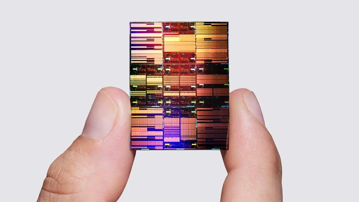
IBM's NanoStack architecture has helped scientists cram 100 billion transistors onto a computer chip, delivering 50% better performance and consuming 70% less energy than the current generation. For the first time, scientists can develop computer chips with transistors smaller than 1 nanometer. The new "NanoStack" architecture that has made this possible could even one day lead to transistors as small as 0.1 nm, the scientists claimed. The new 0.7 nm transistors are significantly smaller than those that feature in standard 2 nm semiconductor chips used in supercomputers, AI systems and advanced graphics processing units (GPUs). While size designation doesn't necessarily correlate with an exact measurement of the transistors on the chips, it does represent their general capabilities. Essentially, the smaller the transistors and their supporting components, the more you can fit on a chip. A typical 2 nm chip design, for example, can fit roughly 50 billion transistors onto a space the size of a human fingernail. The new chip features transistors that are so diminutive they're not measured in nanometers but "angstroms," a unit of measurement typically reserved for atoms. The first of these chips is expected to be manufactured with transistors that are a mere 7 angstroms -- equivalent to 0.7 nanometers or roughly the width of a glucose molecule. At this size, engineers can squeeze nearly 100 billion transistors into a fingernail-size space -- nearly twice that of the current 2 nm platform. Stacking and staggering The scientists achieved this feat using a novel technique called "nanostacking," which they first outlined in a study published as part of the peer-reviewed 2025 Symposium on VLSI Technology and Circuits and uploaded July 2025 to the IEEE Xplore server. This enables engineers to vertically stack the nanosheets used to build the previous generation of 2 nm computer chips. The technology used in all conventional circuits -- known as complementary metal-oxide-semiconductor (CMOS) -- demands extremely high temperatures during manufacturing. As transistors shrink, they also suffer from issues such as "charge trapping" -- where electrons or holes become immobilized by defects or impurities -- and "gate leakage" -- static power dissipation. Such problems have posed a challenge to attempts to shrink transistor size below 2 nm, and thus improve the performance and efficiency of computer chips beyond today's best capabilities. IBM's three-dimensional stacked architecture, however, aims to alleviate some of these pain points, the scientists said. "NanoStack is nanosheets transistors stacking on top of each other. But it's not through a simple monolithic lithography and etch process," said Huiming Bu vice president for IBM semiconductors global R&D and Albany operations, during a press briefing. "What happens here is we actually stack the device. I call it stacking, but also staggering. Stacking in vertical direction, so the front side of each transistor and the backside of each transistor can be contacted independently for signal and power. The stacking of these transistors are done by single dielectric bonding, which is a key innovation that we have developed." IBM representatives added in the briefing that the new technology provides up to 50% greater performance with a 70% reduction in energy use versus the 2 nm platform -- and will eventually replace this technology altogether within the next five years. The scientists say the research could carry deep implications for the computing industry, with revolutionary impacts on the artificial intelligence (AI) and quantum computing sectors. One of the immediate technological benefits could also lie in creating better static random access memory (SRAM) chips, which are used for a variety of computing applications, including CPU caching, networking and in devices such as pacemakers and vehicle sensors. SRAM is also vital in AI processing because it's located close to processing cores (versus other kinds of RAM modules that are often separate components), increasing the speed of data shuttling around systems and therefore reducing bottlenecks. IBM representatives added in the press briefing that they demonstrated a 40% improvement in the scaling of SRAM memory versus the 2 nm platform. This will be a boon to AI workflows, which demand much higher bandwidth and efficiency. The future of computing "We actually have entered a domain that semiconductor manufacturing is almost magic," Huiming added about the design process. "Think about the structure we are building here. We actually deposit the layer atom by atom, and we actually layer atom by atom." IBM representatives said the nanostacking approach isn't a minor upgrade but a generational shift that will eventually enable foundries to scale these chips from 0.7 nm transistors all the way to a single angstrom or just 0.1 nm -- keeping Moore's Law alive for a little longer at least. Shrinking the transistor nodes on these chips will allow for more powerful processes, they said, thanks to a near-twice jump in the transistor count, while the stacked and staggered design significantly reduces the energy requirements. Huiming said that while everybody demands performance, nobody wants to pay the bill for the power. "It will replace nanosheet as today's mainstream [platform] at leading foundries. Whether it's CPU or GPU," he added. "And we believe that transition will happen at around 7 angstroms. So within a decade, this will become another mainstream [platform] that we have invented. This is the next jump in technology." The findings of the 2025 study suggest that not only can the chipset provide much-improved performance with much lower energy consumption, but it may also provide a path toward reducing the thermal impact that high-power computing has on hardware. These innovations could also have an impact on quantum computing, IBM representatives said, as they could lead to improvements in the classical systems with which quantum computers will work together as the technology emerges. "For quantum computing, we need to use lots of classical compute with it," Jay Gambetta, IBM's director of research, said during the press conference. "We want to build decoders, we want to build controllers for decoders and accelerators. And we are working right now on that type of classical with the 2 nm [platform]. If we can continue to change the platform, use more efficient, more powerful [chipsets], it will only help the rate and pace at which we've got to build the classical compute that goes along with the quantum."
[2]
IBM unveils sub-1-nanometer chip architecture that stacks 100 billion transistors onto a fingernail-sized processor
Serving tech enthusiasts for over 25 years. TechSpot means tech analysis and advice you can trust. First look: IBM is once again testing the limits of chip design, this time with an architecture that moves beyond traditional scaling into a more three-dimensional layout aimed at AI workloads. The company refers to the design as a "nanostack" architecture and says it can fit nearly 100 billion transistors onto a chip roughly the size of a human fingernail. That's roughly double the density of IBM's last generation, but the bigger story is how it gets there. Rather than continuing to shrink components along a flat plane, IBM is stacking transistors vertically. That change comes as semiconductor designers run up against the physical limits of traditional scaling, making further miniaturization increasingly difficult and less efficient. In a media briefing covered by Ars Technica, IBM describes the breakthrough as the "world's first sub-1-nanometer chip technology" for AI data centers, though the label is more about performance expectations than literal dimensions. Node names have not corresponded to physical measurements for years. Here, IBM is basically saying the chip behaves like a true sub-1-nanometer design, even though its physical features aren't that small. "It's not just an incremental step, it's a meaningful leap forward," said Jay Gambetta, director of IBM Research and IBM Fellow, in the briefing. He described the new chip technology as "pointing to a future where computing becomes significantly more powerful without a corresponding increase in energy." The architecture builds directly on IBM's earlier work with nanosheet transistors, which formed the basis of its 2-nanometer node introduced in 2021. In the new design, the basic unit consists of two transistors stacked and bonded together. Each transistor is made up of three nanosheets, each about 5 nanometers thick, with roughly 9 nanometers of spacing between them. That layered structure allows IBM to increase transistor density without relying on further horizontal shrinkage, which has become increasingly impractical. In practice, that means it improves performance by building upward rather than just shrinking features sideways. The potential impact on AI infrastructure is a central part of the pitch. According to IBM's projections, the nanostack architecture could deliver up to 50% higher computing performance or 70% better energy efficiency compared with its 2-nanometer chips. For data centers already grappling with power constraints, those kinds of improvements are not incremental. Memory performance is another area where IBM is targeting gains. The company reported a 40% improvement in SRAM scaling, enabled by a staggered-channel design that cuts overall cell height and improves SRAM density. SRAM plays a critical role in AI systems because it supports fast data access, but it has also been one of the hardest components to scale in recent chip generations. "This achievement of 40% will eventually industrialize itself in AI workflows, which require higher bandwidth and high efficiency," Gambetta said. The redesign focuses on SRAM bit cells, each made up of six transistors, allowing more memory to fit within the same footprint. That's important because recent node transitions, including the move from 3-nanometer to 2-nanometer technologies, have delivered only modest improvements in SRAM scaling. IBM's role in all of this remains rooted in research rather than manufacturing. The company typically works with partners to bring its designs to market. It has collaborated with Rapidus in Japan on 2-nanometer production and with Samsung on related semiconductor advances. At the same time, other major players, such as TSMC, have independently adopted nanosheet transistor designs, reflecting how IBM's research tends to influence the broader industry. "Nanosheet has become the foundation of the next generation of transistor scaling," said Huiming Bu, vice president of IBM Semiconductors Global R&D and IBM Research. "Today, nanosheet is adopted by all leading foundries for most of the 3-nanometer chips and all of the 2-nanometer chips." Looking ahead, IBM has not named partners for commercializing the nanostack architecture, but it expects the technology to reach production within the next decade, possibly sooner. Bu said the design is positioned to replace nanosheet architectures as the industry standard across processors, including CPUs and GPUs. "It will replace nanosheet as today's mainstream in leading foundries, whether it's CPUs or GPUs," Bu said. "Within a decade, this will become another mainstream that we have invented and helped industry to transform."
[3]
IBM announces world's first sub-1 nanometer chip with nanostack technology doubling transistor density
IBM has announced what it calls the world's first sub-1 nanometer chip technology, unveiling a new 0.7nm process built around an entirely new transistor architecture called nanostack. The result is a chip the size of a human fingernail that packs nearly 100 billion transistors, almost double the density of IBM's previous 2nm chip from 2021. IBM says the architecture could deliver either 50% higher performance or 70% greater energy efficiency compared to its predecessor, and it represents what the company believes is a viable path for chip scaling for at least the next decade. Before going ahead, it is worth clarifying what "sub-1 nanometer" actually means here. Modern process node names have not corresponded to literal physical dimensions for decades. IBM's 0.7nm designation, which it also calls the 7 angstrom node, refers to a generation of manufacturing capability rather than a physical transistor size. What matters practically is that the architecture delivers the density and efficiency improvements that such a node implies. The nanostack architecture builds on IBM's existing nanosheet transistor technology, which it introduced with its 2nm chip in 2021 and which has since been adopted by TSMC, Samsung, and other leading foundries as the foundation for their own advanced nodes. Rather than continuing to shrink transistors horizontally, nanostack stacks and staggers transistors vertically in a three-dimensional layout. Each transistor consists of three nanosheet elements, approximately five nanometers thick with nine nanometers between each layer, and each nanosheet is made up of roughly 15 rows of silicon atoms. IBM also says the architecture allows different material combinations within stacked layers, potentially letting engineers optimize individual layers independently for performance, power, or other characteristics. IBM researchers demonstrated a 40% improvement in SRAM scaling using the nanostack architecture, the largest such improvement in roughly a decade. Between the 3nm and 2nm generations, SRAM scaling improved by only a few percent. The jump matters because SRAM is used for processor cache, and AI workloads are increasingly constrained by memory bandwidth and efficiency. Jay Gambetta, director of IBM Research, said the SRAM result will eventually be industrialized for AI workflows that require higher bandwidth and efficiency. With our new nanostack architecture, we're not just making smaller transistors," Gambetta said. "We're reinventing how chips are built to deliver dramatically more power and energy efficiency. IBM estimates nanostack chips could enter production within five years, though the company has not named specific manufacturing partners. Its previous nanosheet technology is being commercialized by Rapidus in Japan, which is targeting production of 2nm chips at scale by the second half of 2027. IBM has said it will share more details on commercialization plans in the future.
[4]
IBM Unveils World's First Sub-1nm Chip Technology, New Era for AI Computing Begins
IBM has developed the world's first sub-1nm chip technology that could revolutionize semiconductor research. The advancement would not only make AI computations faster but would also help to develop advanced processor technology. The announcement comes as chipmakers look for new ways to sustain the pace of innovation described by Moore's Law, the principle proposed by Intel co-founder Gordon Moore that the number of transistors on a chip would roughly double every two years. The prototype, built on a 0.7nm (7 angstroms) process, uses a new three-dimensional Nanostack architecture that vertically stacks transistors rather than relying solely on shrinking them. said the technology is designed to support increasingly demanding workloads in artificial intelligence (AI), cloud computing, and high-performance computing. As transistors approach atomic dimensions, continuing that trend through conventional scaling has become increasingly difficult because of power, heat, and manufacturing constraints. "The next frontier of semiconductor innovation isn't just about making things smaller, it's about rethinking how chips are built from the ground up," . The company said the technology marks the beginning of semiconductor development, where transistor dimensions are measured in angstroms rather than nanometres. One angstrom is one-tenth of a nanometre, making the new technology a 7-angstrom node. To illustrate the scale, IBM noted that a human red blood cell is about 7,000 nanometres wide, roughly 10,000 times larger than the chip's 0.7nm transistor node.
Share
Copy Link
IBM has developed the world's first sub-1nm computer chip using a revolutionary nanostack architecture that vertically stacks transistors. The fingernail-sized chip packs nearly 100 billion transistors—double the density of current 2nm chips—while delivering 50% better performance and 70% improved energy efficiency. This breakthrough could reshape AI computing and semiconductor manufacturing over the next decade.
IBM Breaks Barrier with World's First Sub-1nm Computer Chip
IBM has achieved a significant milestone in semiconductor manufacturing by developing the world's first sub-1nm computer chip, marking a new era where transistor dimensions are measured in angstroms rather than nanometers . The company's innovative nanostack architecture enables engineers to pack nearly 100 billion transistors onto a fingernail-sized chip—almost double the density of IBM's previous 2nm chips from 2021
3
. Built on a 0.7nm process, equivalent to 7 angstroms or roughly the width of a glucose molecule, this breakthrough demonstrates that chip innovation can continue even as the industry approaches atomic-scale dimensions .
Source: Analytics Insight
Vertical Stacking Transistors Solves Critical Manufacturing Challenges
The nanostack architecture fundamentally reimagines chip design by stacking and staggering transistors vertically rather than continuing to shrink components along a flat plane . Each transistor consists of three nanosheet elements, approximately 5 nanometers thick with 9 nanometers of spacing between each layer, and each nanosheet comprises roughly 15 rows of silicon atoms
3
. This three-dimensional approach addresses longstanding issues like charge trapping—where electrons become immobilized by defects—and gate leakage, which causes static power dissipation . "NanoStack is nanosheets transistors stacking on top of each other," explained Huiming Bu, vice president for IBM semiconductors global R&D, noting that the stacking is achieved through single dielectric bonding, allowing the front and back sides of each transistor to be contacted independently for signal and power .Dramatic Performance Gains Target AI Computing Demands
IBM projects the nanostack architecture could deliver up to 50% higher computing performance or 70% better energy efficiency compared to 2nm chips—a critical advancement for AI workloads that demand higher bandwidth and efficiency . For data centers already grappling with power constraints, these improvements represent a meaningful leap forward. "It's not just an incremental step, it's a meaningful leap forward," said Jay Gambetta, director of IBM Research, describing the technology as "pointing to a future where computing becomes significantly more powerful without a corresponding increase in energy" . The architecture also demonstrated a 40% improvement in SRAM scaling—the largest such improvement in roughly a decade—which matters because SRAM is located close to processing cores and supports fast data access critical for AI systems
3
.
Source: TechSpot
Related Stories

Path to Production and Industry Transformation
IBM expects the technology to reach production within five years and potentially replace nanosheet transistors as the industry standard within a decade
3
. While IBM has not named specific manufacturing partners for commercializing the nanostack architecture, the company has previously collaborated with Rapidus in Japan on 2nm production and with Samsung on semiconductor advances . The research, first outlined in a study published as part of the peer-reviewed 2025 Symposium on VLSI Technology and Circuits, suggests the approach could eventually enable foundries to scale chips all the way to a single angstrom or 0.1nm, keeping Moore's Law alive for longer . "Nanosheet has become the foundation of the next generation of transistor scaling," Bu noted, adding that the design is positioned to become mainstream across processors, including CPUs and GPUs . The breakthrough carries deep implications not just for AI computing but also for quantum computing sectors, as the industry continues to push against the physical limits of traditional scaling4
.
Source: Live Science
References
Summarized by
Navi
[1]
[3]
[4]
Related Stories
Stanford team builds first commercial 3D chip at US foundry with 4x AI performance gains
14 Dec 2025•Science and Research
Breakthrough in Neuromorphic Computing: Single Silicon Transistor Mimics Neuron and Synapse
29 Mar 2025•Technology
Fujitsu and Rapidus partner to build 1.4nm AI chip entirely in Japan with government backing
31 Mar 2026•Technology

Recent Highlights
1
OpenAI and Broadcom unveil Jalapeño chip to power next-generation AI inference at scale
Technology

2
Anthropic faces AI export ban as Mythos reportedly breached NSA systems in hours
Policy and Regulation

3
Meta launches AI-powered glasses at $299, ditching Ray-Ban to expand smart glasses market
Technology

Recent Highlights
Today's Top Stories


Don’t drown in AI news. We cut through the noise - filtering, ranking and summarizing the most important AI news, breakthroughs and research daily. Follow topics that matter to you and stay ahead.


