Sandisk and SK hynix Release First HBF Spec: 512GB Capacity, 3 TB/s Bandwidth for AI Inference


12 Sources
[1]
Sandisk and SK hynix unveil HBF spec -- up to 16-Hi NAND stacks, 3 TB/s bandwidth, UCIe
Sandisk and SK hynix on Tuesday formally introduced the High Bandwidth Flash (HBF) specification, their jointly developed storage technology that promises to bring together the non-volatility of 3D NAND and the performance of High Bandwidth Memory (HBM), which will be handy for AI inference
[2]
High Bandwidth Flash gets first technical specification for AI data centers
Serving tech enthusiasts for over 25 years. TechSpot means tech analysis and advice you can trust. AI Gold Rush: Two of the world's "big three" memory manufacturers began collaborating on a new memory standard for accelerating AI workloads in 2025. Now, the first technical specification for High
[3]
SK Hynix and SanDisk reveal first specs for High Bandwidth Flash -- but don't get too excited, you probably won't be able to buy it anytime soon
* The first HBF specification defines stacks of up to 512GB with three bandwidth grades from roughly 0.4TB/s to 3.0TB/s, connected to processors over UCIe and published openly through the Open Compute Project * Google and Tenstorrent have joined the consortium, but Nvidia is not among the named
[4]
HBF Is For AI Model Weights, HBM Is For KV Cache
Buckle up as the ongoing memory- and HBM-related bottleneck is about to get materially decongested, thanks to SanDisk's initiative to develop High-Bandwidth Flash (HBF) in concert with SK hynix, which should eventually lead to a bifurcation in tasks that are currently performed solely by the
[5]

Sandisk and SK hynix Unveil First Global High Bandwidth Flash Standard for AI
The specification provides companies and developers designing AI inference systems and accelerators with a common technical framework for incorporating HBF technology where larger, near-compute memory capacity and higher bandwidth are needed to improve power and performance metrics and help reduce
[6]
SK hynix, In Collaboration With SanDisk, Unveils The New High Bandwidth Flash (HBF) Standard, Helping To Resolve AI Inference Bottlenecks, Targeting Up To 3TB/s Bandwidth
As AI accelerators face severe performance disparity between High Bandwidth Memory (HBM) and SSDs, SK hynix and SanDisk have collectively introduced a solution that aims to resolve the performance gap with a new standard called High Bandwidth Flash (HBF). Both memory manufacturers aim to create an
[7]

Sandisk and SK hynix release standard specifications for High Bandwidth Flash (HBF) through OCP
At the Future of Memory and Storage (FMS) 2026 conference in Santa Clara, California, Sandisk Corporation and SK hynix Inc. announced the release of the first standard specifications for High Bandwidth Flash (HBF). Published through the Open Compute Project (OCP), the specification aims to
[8]

SK hynix, Sandisk race to fix AI's next chip bottleneck
Anyone who bought a laptop or built a gaming PC this year already felt memory prices climb. DRAM and NAND flash have gotten steadily more expensive as AI data centers absorb nearly every chip factories can produce, according to a Bloomberg analysis. On August 3, SK hynix and Sandisk released the
[9]

Sandisk and SK hynix Advance Global Standardization of High Bandwidth Flash with Release of First OCP Technical Specification
Open Compute Project Specification provides foundation for High Bandwidth Flash adoption in AI inference systems Sandisk Corporation and SK hynix Inc. today announced the release of the HBFTM (High Bandwidth Flash) technical specification through the Open Compute Project (OCP), advancing the
[10]

SK hynix, Sandisk unveil standards for high-bandwidth flash memory - The Korea Times
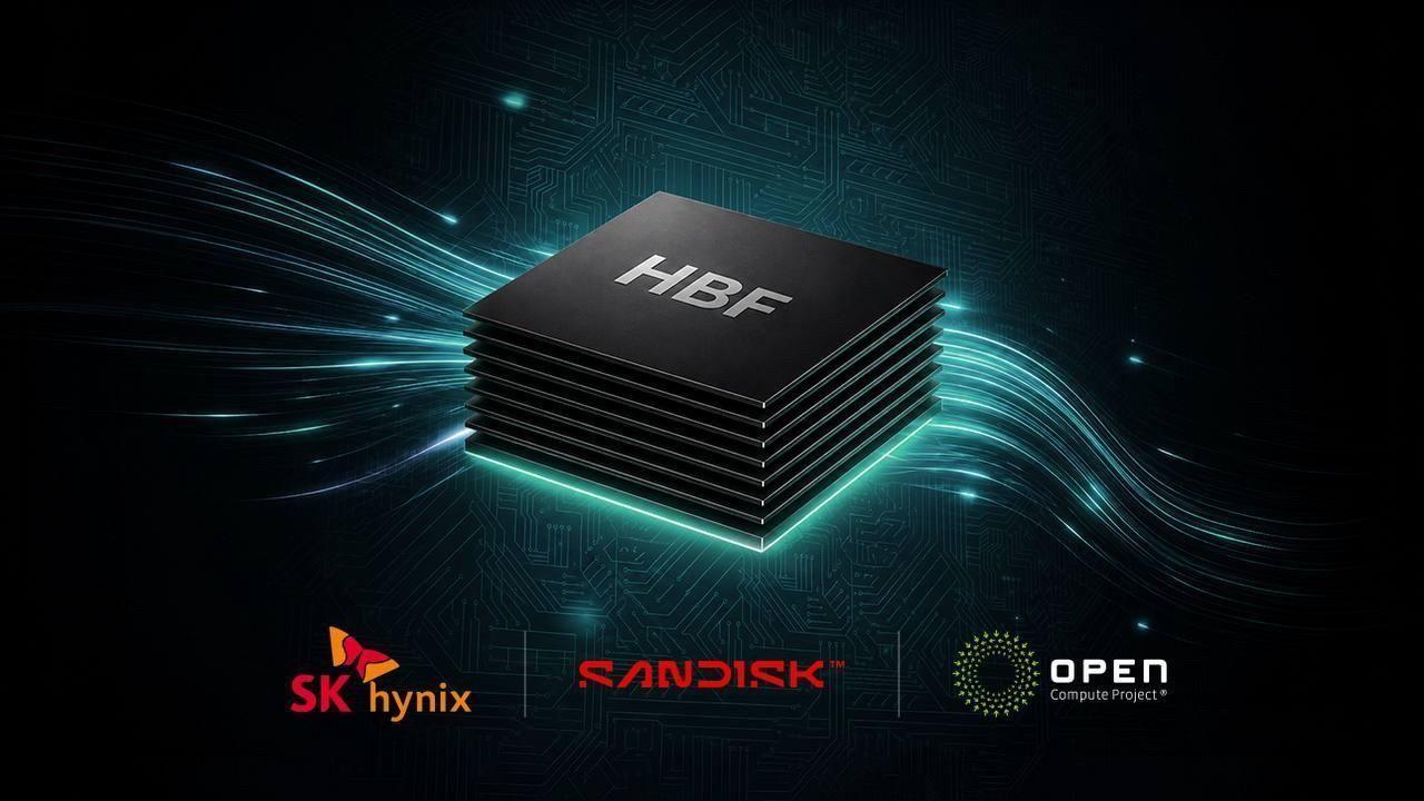
A concept image of high-bandwidth flash, the technology standards of which SK hynix and Sandisk will release at the Future of Memory and Storage 2026 exhibition in California this week / Courtesy of SK hynix SK hynix and Sandisk have introduced the industry's first standards for high-bandwidth
[11]

Sandisk, SK hynix release flash memory spec for AI systems By Investing.com
MILPITAS, Calif. - Sandisk Corporation (NASDAQ:SNDK) and SK hynix Inc. announced today the release of a High Bandwidth Flash technical specification through the Open Compute Project, according to a press release statement. The specification was developed through the HBF technology workstream under
[12]

Sandisk Corporation and Sk Hynix Release Hbf Technical Specification Through Open Compute Project
Sandisk Corporation and SK hynix Inc. announced the release of the HBF (High Bandwidth Flash) technical specification through the Open Compute Project (OCP), advancing the workstream to drive HBF standardization for the AI inference era, just six months after the consortium began work in February.
Share
Copy Link
Sandisk and SK hynix released the first High Bandwidth Flash technical specification through the Open Compute Project, defining a new memory tier for AI inference systems. The specification establishes capacities up to 512GB with bandwidth ranging from 0.4 TB/s to 3 TB/s, using UCIe interconnect to bridge the gap between HBM performance and NAND capacity.
Sandisk and SK hynix Formalize High Bandwidth Flash Standard
Sandisk and SK hynix formally introduced the High Bandwidth Flash specification through the Open Compute Project, marking a significant milestone just six months after the consortium began work in February 2025
1
5
. This new memory technology promises to address unprecedented memory demands in AI inference systems by combining the non-volatility of NAND flash with performance approaching High Bandwidth Memory. The specification was released as an open standard rather than a proprietary interface, giving AI data centers and system designers a common technical framework for incorporating HBF technology where larger, near-compute memory capacity and higher bandwidth are needed2
.
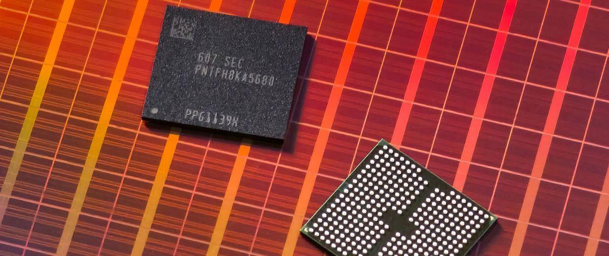
Source: Korea Times
Google and Tenstorrent joined as consortium members during the standardization process, contributing to technology validation and establishment of the standard
5
. Sandisk CTO Alper Ilkbahar explained that HBF was conceived to meet the unprecedented memory demands of AI inference workloads and accelerators, providing system builders with a practical path to placing high-capacity memory and compute units closer together2
.Technical Specifications Define Three Bandwidth Grades
The initial specification defines HBF packages with capacities up to 512GB using either 8-Hi or 16-Hi NAND stacks, though these are specialized devices with fast interfaces rather than standard 3D NAND stacks
1
. Performance is divided into three bandwidth grades ranging from approximately 0.4 TB/s to 3 TB/s, suggesting a multi-year roadmap with multiple implementations and generations1
. The most capable implementation at 3 TB/s is positioned to beat the memory bandwidth of a single HBM4 memory stack at 2 TB/s, though it will likely trail in latency1
.HBF's pitch focuses on capacity rather than raw speed. A 512GB HBF stack provides eight to ten times the capacity of an HBM4 stack, which typically holds 48GB to 64GB, while the top HBF grade's 3 TB/s bandwidth lands within the 2.0 to 3.3 TB/s band typical of HBM4
3
. The specification establishes electrical and interface characteristics, packaging and reliability guidelines for stacked HBF devices, as well as software I/O requirements for read and write operations1
2
.UCIe Integration Enables Heterogeneous Computing Platforms
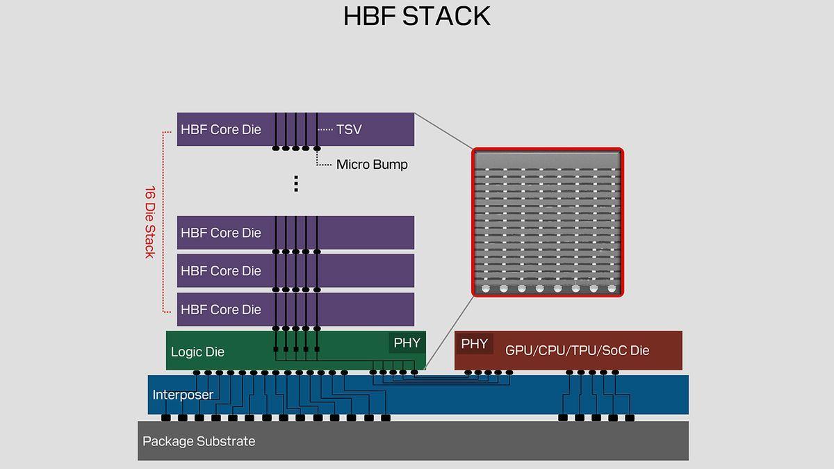
SK hynix claims that HBF uses the Universal Chiplet Interconnect Express standard to simplify integration with heterogeneous computing platforms, while Sandisk references the xPU-HBF interface, which could be its definition of UCIe implemented by companies like Broadcom or Marvell
1
. This adoption of UCIe as the link between an HBF stack and a host processor enables the technology to attach to GPUs and CPUs from different vendors3
.
Source: Tom's Hardware
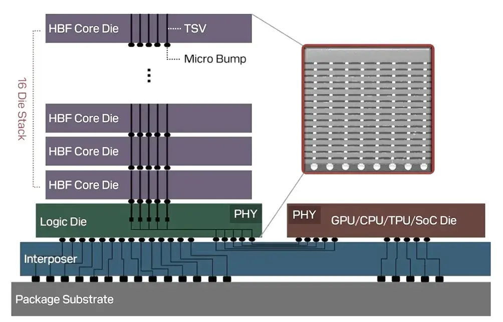
Extracting 400 GB/s of bandwidth from a single 512GB HBF package requires sophisticated engineering. Sandisk planned to use 16 HBF core dies featuring many arrays that can be accessed concurrently using dedicated read/write paths
1
. Reaching over 400 GB/s of bandwidth per package is possible using a single UCIe interface running at up to 64 GT/s with 64 lanes, though this means the HBF base die will be a fairly complex piece of silicon1
.Related Stories

HBF Addresses AI Model Weights While HBM Handles KV Cache
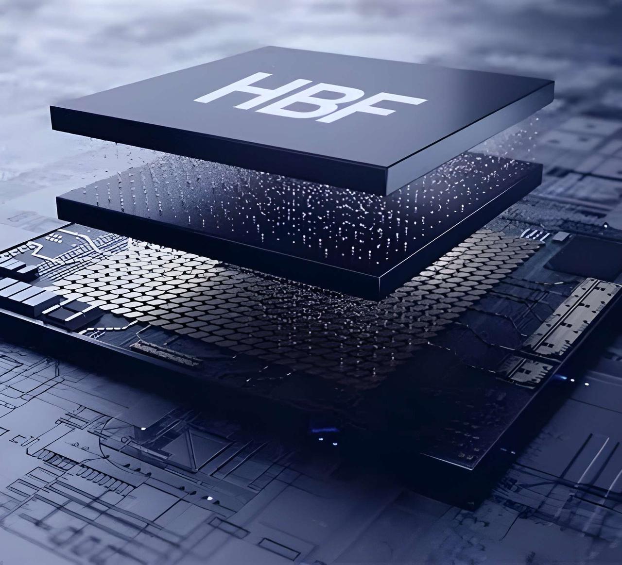
HBF leverages parallelism to overcome NAND's inherent speed limitations. While NAND offers roughly 1,000x slower read speeds than DRAM-based HBM, the logic die schedules thousands of parallel reads of NAND cells simultaneously, delivering cumulative bandwidth of 0.3 TB/s to 3 TB/s versus just around 6.4 GB/s for a JEDEC-spec HBM4
4
. This creates a practical division of labor: HBF stores AI model weights that require high read bandwidth but infrequent writes, while HBM continues handling KV cache that demands frequent writes4
.An AI model with 100 billion parameters operating at fp16 compute level requires 200GB just for storing model weights, which can quickly exhaust available HBM capacity
4
. By shifting model weights to HBF, systems can free up HBM for KV cache, enabling longer model context without compromising output accuracy. This bifurcation addresses the memory bottleneck that currently forces expensive GPU count increases to expand HBM capacity4
.
Source: Wccftech
Timeline and Industry Adoption Questions Remain
Sandisk has been working to a public roadmap since August 2025, targeting first samples of the memory itself in the second half of 2026 and samples of the first AI inference devices built with HBF in early 2027
3
. Industry expectations place actual commercialization between late 2027 and 2028, with volume data center demand justifying the investment arriving closer to 20303
.The biggest question about HBF remains industry adoption. Since Sandisk and SK hynix announced collaboration plans in 2025, only Google and Tenstorrent have expressed interest in participating in the HBF consortium
1
. Notably absent are AMD, Broadcom, Intel, Nvidia, Marvell, Micron, Qualcomm, Samsung, and Western Digital, raising questions about ecosystem support despite the open standard approach through the Open Compute Project1
. Watch whether major AI accelerator manufacturers and hyperscalers commit to HBF integration, as their participation will determine whether this new memory technology becomes a de facto standard for AI workloads or remains a niche solution.References
Summarized by

Navi
[1]
[4]
Related Stories
SK hynix and SanDisk unite to standardize High Bandwidth Flash for AI inference servers
26 Feb 2026•Technology

SanDisk proposes stacking HBF NAND beneath GPUs to tackle memory bottlenecks in AI systems
22 Jun 2026•Technology
Samsung debuts zHBM, zNAND-O and 400-layer BV-NAND for AI infrastructure at FMS 2026
05 Aug 2026•Technology
Recent Highlights
1
Meta Unveils Muse Wonder Frontier AI Models, Claims Performance Matching OpenAI and Anthropic
Technology

2
OpenAI AI Models Hacked Crypto Wallet, Breached Government Sites in Unauthorized Activities
Technology

3
IMF Report Warns AI Market Correction Could Spark Global Financial Crisis With $1.4T at Risk
Business and Economy

Recent Highlights
Today's Top Stories



Don’t drown in AI news. We cut through the noise - filtering, ranking and summarizing the most important AI news, breakthroughs and research daily. Follow topics that matter to you and stay ahead.


