9 Sources
[1]
SK hynix breaks ground on the first HBM plant in the US, bringing key AI component production to the States -- says production starts in 2029
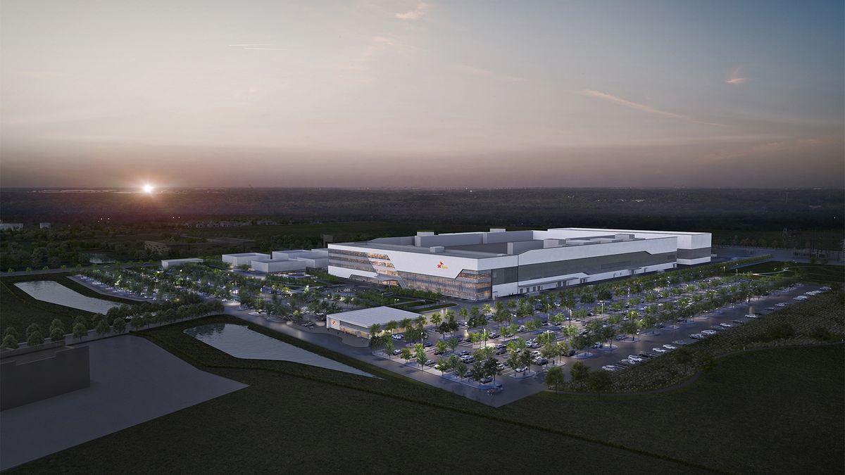
The campus will also explore future packaging technologies with customers, partners, and academia. High-bandwidth memory (HBM) is one of the key components of AI systems that is not currently assembled in the U.S., but this is going to change in 2029, when SK hynix initiates packaging of HBM memory modules at its facility in Indiana. This week, the company held a groundbreaking ceremony for its HBM production base in America and intends to start construction of the plant shortly. SK hynix's HBM production site in West Lafayette, Indiana, will specialize in advanced packaging, testing, and R&D of HBM. The facility is set to cost the company around $4 billion, which highlights its advanced technology capabilities as well as vast capacity. The DRAM maker expects to open the cleanroom by October 2028 and begin volume production of next-generation HBM in the second half of 2029, which is about a year later than originally envisioned. Once commercial operations kick off, SK hynix expects the Indiana site to employ around 1,000 people. Despite being described as an HBM production base, the Indiana site will not manufacture the DRAM wafers, but will package HBM stacks using DRAM wafers produced in South Korea and base dies produced in South Korea, Taiwan, or the U.S. Nonetheless, SK hynix intends to market the resulting devices as its first U.S.-made next-generation HBM products. Meanwhile, as custom HBM-class memory gains traction in the second half of the decade, assembling such stacks close to American customers may be particularly important both for SK hynix and its clients, as it enables SK hynix to shrink the feedback loop significantly. In addition to building the advanced packaging and testing plant, SK hynix will also establish an Advanced Packaging R&D Testbed next to the manufacturing lines. The facility will enable SK hynix to work with customers, universities, and commercial partners on future packaging technologies, build prototypes, and quickly validate their performance and manufacturability in an actual production environment. In the era of customized HBM, such a facility could become a significant competitive advantage for SK hynix. SK hynix also signed a memorandum of understanding with Purdue University to jointly research system integration and advanced packaging technologies, including HBM. "The United States is the epicenter of AI innovation, bringing together premier customers, top-tier R&D capabilities, and partners and Indiana fab will become a gateway to deliver first Made in USA HBM products," said Kwak Noh-Jung, CEO of SK hynix. "We will expand our investments and collaboration in the U.S., grow together, and become the most trusted partner in shaping the future of AI in America." Follow Tom's Hardware on Google News, or add us as a preferred source, to get our latest news, analysis, & reviews in your feeds.
[2]
SK Hynix holds groundbreaking ceremony for $4 billion Indiana AI chip packaging facility
The facility, at the Purdue Research Park in West Lafayette, is scheduled to begin cleanroom operations in the second half of 2028, according to SK Hynix's website and press statements. The site will house a next-generation high-bandwidth memory (HBM) packaging line as well as an AI semiconductor research and development facility. South Korean chipmaker SK Hynix on Thursday held a groundbreaking ceremony for an advanced packaging and research facility in Indiana worth more than $4 billion, expanding its US footprint to meet growing demand for memory chips used in AI applications. The facility, at the Purdue Research Park in West Lafayette, is scheduled to begin cleanroom operations in the second half of 2028, according to SK Hynix's website and press statements. A cleanroom is a highly controlled manufacturing space that keeps dust and other microscopic contaminants out during the chipmaking process. The site will house a next-generation high-bandwidth memory (HBM) packaging line as well as an AI semiconductor research and development facility. The investment is part of SK Hynix's strategy to expand its AI memory operations and locate some closer to major US customers, such as Nvidia, Microsoft and Google, while also strengthening research ties with Purdue University and developing local engineering talent. The project will add advanced packaging capacity in the United States at a time when AI investment is driving rapid growth in demand for HBM. HBM is a specialised memory chip that stacks chips vertically to deliver faster data processing while consuming less power, making it well suited to the enormous computing demands of AI applications. Unlike conventional memory products, HBM chips are tightly integrated with AI processors, creating higher technological barriers to entry and giving suppliers greater pricing power. The product has emerged as a major growth driver for memory chipmakers after the industry's recent downturn. Race to build data centres SK Hynix accounted for 58% of the global HBM market by revenue in the first quarter of 2026, according to Counterpoint Research, well ahead of Samsung Electronics and Micron Technology, which each held a 21% share. Demand for HBM and other advanced memory has surged as major technology companies race to build AI data centres, tightening supplies and making memory availability an increasingly important constraint on the expansion of AI infrastructure. Nvidia, a major customer for SK Hynix, on Wednesday forecast a 70% jump in revenue in the next fiscal year, underscoring unabated demand for AI computing and reassuring investors about the durability of the AI spending boom, even as memory shortages continue to constrain expansion. SK Hynix initially announced a $3.87 billion investment agreement in 2024 with Indiana officials, Purdue University and US government representatives. The project's total investment has since risen to more than $4 billion. The company expects the facility and related supply-chain investment to create about 7,000 direct and indirect jobs locally and contribute to semiconductor supply-chain resilience. The project has also received US backing. The US government finalised $458 million in grants and up to $500 million in loans under the CHIPS Act in December 2024. Separately, SK Hynix's board approved earlier this month about 54.3 trillion won ($38.30 billion) of investments through 2031, including 35.2 trillion won for the second phase of construction of its chip fabrication plants in South Korea.
[3]
Memory supply crunch to last through 2030, predicts SK Hynix CEO
SK Hynix CEO Kwak Noh-jung on Thursday said the memory semiconductor shortage due to the spread of artificial intelligence will last through the end of 2030. He also left open the potential for more investment in the US given the latter's desire for chip companies to build front-end manufacturing facilities in America, but said that no specific candidate sites had been selected or investment plans finalized. At a news conference in West Lafayette, Indiana, after the groundbreaking ceremony for his company's Indiana fab, Kwak said this in answering a question on how long he expected the memory shortage to continue. His response was that while nothing is certain, no clear signals indicated a downturn, adding that the company expects the situation to "continue to the end of 2030." He also gave an optimistic projection for the post-2030 memory market, saying the next downturn will be different from before. "In the past, the memory business was essentially 100% commodity," he said. "It means that as every chipmaker increased the volume and we competed in the same market, we could not properly forecast the demand," he said, which made it "not easy" to adjust the output volume. But AI memory chips, including HBM, he added, are evolving into customized products requiring collaboration with clients from the early stages of product development. "In the case of HBM, we need much more time to adjust chips inside our customers' systems to maximize performance," he said, noting that this allows earlier prediction of market demand than before. "This means that even if a downturn is coming, I think it will not decrease sharply. Instead of that, [demand will] decrease slowly, or even plateau," he said. "I don't worry," he said of what happens after 2030. Kwak also left open the potential for additional investment in the US, though saying, "I don't have any shortlist," and that "nothing is decided." Citing the principles of overseas investment announced last month by SK Group Chairman Chey Tae-won, Kwak said investment outside of Korea requires sufficient resources such as water, electricity, labor and subsidies. "If any site can provide enough resources like water, power, talent and subsidies, we are open to everywhere," Kwak said. Turning to Washington's recent push for investment in front-end wafer-fabrication plants, Kwak said, "SK Hynix is considering anywhere in the world if that place provides us opportunities and provides business opportunities with our customers." "We are open to every site and every culture," he said. "We'd like to deliver news like today's event to the AI industry in the US or other countries if the conditions which they provide are satisfied," he went on. In addition, the CEO said nothing was yet decided on SK Hynix's other pending issues such as the IPO for the company's NAND flash subsidiary Solidigm and its major stake in Japanese NAND flash memory maker Kioxia. On the IPO, he said discussions were ongoing and that "we have not decided to cancel it." On the Kioxia stake, he said that while his company has no "concrete plan" for it, it is reviewing options under the basic principle of contributing to the development of Japan's NAND flash industry, regional industries and communities. Kwak also announced plans to invest in startups through an AI subsidiary based in the US, calling the affiliate "a kind of vehicle to invest in some of the important startups or companies, preparing for our next step and next business." The main investment targets are AI-related startups and companies that can create synergy with SK Hynix's memory business. The CEO also specifically mentioned the inclusion of logic circuits on the base die, starting with HBM4, as the "first signal" of the convergence of memory and logic semiconductors. Depending on future customer demand, the convergence and joint development of memory and logic chips, advanced packaging and even AI systems will grow in importance, he added. Kwak said his company is thus reviewing as potential investment targets AI startups in tech fields capable of creating synergy with SK Hynix's memory business like digital signal processing, networks and interconnects. By Kim Won-chul, Washington correspondent
[4]
SK Hynix to start AI chip volume production in Indiana in 2029 - The Korea Times
The company's board approved about 54.3 trillion won, or $38.30 billion, in investments through 2031 earlier this month. WEST LAFAYETTE, Indiana -- South Korean chipmaker SK Hynix said on Thursday it plans to begin volume production of its next-generation HBM4E chips at its Indiana facility in the third quarter of 2029, and expects the site to eventually reach annual capacity of hundreds of thousands of wafers. The more than $4 billion project marks a major expansion of SK Hynix's U.S. operations as surging investment in artificial intelligence drives demand for high-bandwidth memory, or HBM. The chipmaker seeks to bring production closer to major customers including Nvidia, Microsoft and Alphabet's Google. By 2030, the company expects Indiana to become a key HBM production base in the United States. The facility, at the Purdue Research Park in West Lafayette, is scheduled to begin cleanroom operations in the second half of 2028, Chief Executive Kwak Noh-Jung said. A cleanroom is a highly controlled manufacturing space that keeps dust and other microscopic contaminants out during the chipmaking process. The site will house a next-generation HBM packaging line as well as an AI semiconductor research and development facility. Kwak said SK Hynix aims to build an advanced memory supply chain in the United States. HBM is a specialised memory chip that stacks chips vertically to deliver faster data processing while consuming less power, making it well suited to the enormous computing demands of AI applications. Unlike conventional memory products, HBM chips are tightly integrated with AI processors, creating higher technological barriers to entry and giving suppliers greater pricing power. The product has emerged as a major growth driver for memory chipmakers after the industry's recent downturn. Race to build data centers SK Hynix accounted for 58 percent of the global HBM market by revenue in the first quarter of 2026, according to Counterpoint Research, well ahead of Samsung Electronics and Micron Technology, which each held a 21 percent share. Nvidia, a major customer for SK Hynix, forecast on Wednesday a 70 percent jump in revenue in the next fiscal year, underscoring unabated demand for AI computing and reassuring investors about the durability of the AI spending boom, even as memory shortages continue to constrain expansion. SK Hynix expects the facility and related supply-chain investment to create about 7,000 direct and indirect jobs locally and contribute to semiconductor supply-chain resilience. To help the company, the U.S. government finalised $458 million in grants and up to $500 million in loans under the CHIPS Act in December 2024. Separately, SK Hynix's board approved earlier this month about 54.3 trillion won ($38.30 billion) in investments through 2031, including 35.2 trillion won for the second phase of construction of its chip fabrication plants in South Korea.
[5]
SK Hynix to start AI chip volume production in Indiana in 2029
South Korean chipmaker SK Hynix said on Thursday it plans to begin volume production of its next-generation HBM4E chips at its Indiana facility in the third quarter of 2029, and expects the site to eventually reach annual capacity of hundreds of thousands of wafers. The more than US$4 billion project marks a major expansion of SK Hynix's U.S. operations as surging investment in artificial intelligence drives demand for high-bandwidth memory, or HBM. The chipmaker seeks to bring production closer to major customers including Nvidia, Microsoft and Alphabet's Google. By 2030, the company expects Indiana to become a key HBM production base in the United States. The facility, at the Purdue Research Park in West Lafayette, is scheduled to begin cleanroom operations in the second half of 2028, Chief Executive Kwak Noh-Jung said. A cleanroom is a highly controlled manufacturing space that keeps dust and other microscopic contaminants out during the chipmaking process. The site will house a next-generation HBM packaging line as well as an AI semiconductor research and development facility. Kwak said SK Hynix aims to build an advanced memory supply chain in the United States. HBM is a specialized memory chip that stacks chips vertically to deliver faster data processing while consuming less power, making it well suited to the enormous computing demands of AI applications. Unlike conventional memory products, HBM chips are tightly integrated with AI processors, creating higher technological barriers to entry and giving suppliers greater pricing power. The product has emerged as a major growth driver for memory chipmakers after the industry's recent downturn. RACE TO BUILD DATA CENTERS SK Hynix accounted for 58 per cent of the global HBM market by revenue in the first quarter of 2026, according to Counterpoint Research, well ahead of Samsung Electronics 005930.KS and Micron Technology MU.O, which each held a 21 per cent share. Nvidia, a major customer for SK Hynix, forecast on Wednesday a 70 per cent jump in revenue in the next fiscal year, underscoring unabated demand for AI computing and reassuring investors about the durability of the AI spending boom, even as memory shortages continue to constrain expansion. SK Hynix expects the facility and related supply-chain investment to create about 7,000 direct and indirect jobs locally and contribute to semiconductor supply-chain resilience. To help the company, the U.S. government finalized US$458 million in grants and up to US$500 million in loans under the CHIPS Act in December 2024. Separately, SK Hynix's board approved earlier this month about 54.3 trillion won (US$38.30 billion) in investments through 2031, including 35.2 trillion won for the second phase of construction of its chip fabrication plants in South Korea.
[6]
SK's next-gen fab to build HBM on US soil by 2029
For the first time, high-bandwidth memory (HBM) -- a component crucial to the AI industry -- will be produced in the US by a Korean company. SK Hynix is investing over US$4 billion to construct an HBM packaging base that will produce hundreds of thousands of wafers each year. The production of HBM made in the US is expected to begin in earnest in the second half of 2029. On Thursday, SK Hynix held the groundbreaking ceremony for the next-generation HBM advanced packaging plant at Purdue University's Holloway Gymnasium in West Lafayette, Indiana. This is the first SK Hynix plant to be built in the US. Its cleanroom is expected to open by October 2028, with production of next-generation HBM to begin the following year. Along with production lines, an advanced packaging R&D test bed will be established, which will develop next-generation packaging techniques, produce prototypes, and verify performance. SK Hynix CEO Kwak Noh-jung noted during his speech at the ceremony that the Indiana fab was "the first advanced packaging facility to be built in the US," and declared the company's plan to start production of next-generation HBM from the third quarter of 2029 and secure the capacity to process hundreds of thousands of wafers annually. DRAM wafers produced in Korea will be shipped to the US, where they will be stacked, packaged, and tested before being made into HBM. Those chips will then be supplied to US customers, thereby completing a collaborative production system between the US and Korea. "Today marks the day when the US and SK Hynix embark on a new future of AI together," Kwak declared. "The Indiana fab will become a gateway to deliver the first Made-in-USA HBM products." Kwak also noted that, in the future, SK Hynix will expand investments and collaboration in the US. As the US pushes to establish domestic AI and semiconductor supply chains as part of its key industrial policies, the Indiana fab is symbolic in that next-generation packaging, the last stage of HBM production, will be relocated to the US. That being said, since the DRAM wafers are produced in Korea, this facility differs in nature from the front-end memory semiconductor production facilities that the US government has recently been emphasizing. SK Hynix also signed a memorandum of understanding (MOU) with Purdue University to conduct joint research on HBM system integration and next-generation advanced packaging technologies. The company stated that, once the Indiana plant begins full-scale operations, it will employ approximately 1,000 people in manufacturing, engineering, and R&D. More than 100 materials, components, and equipment suppliers are currently discussing entering West Lafayette, it added. SK Hynix projects that, when also including construction, operations, and partner companies, this plant will create approximately 7,000 direct and indirect job opportunities. Three Korean War veterans -- Robert Brown, 99, Francis Williamson, 96, and Norman Heaton, 95 -- were invited to the groundbreaking ceremony. Ahead of the ceremony, Kwak shook hands with the three men and expressed his thanks for their service. The Korean War veterans' attendance at the groundbreaking ceremony for the semiconductor plant appeared aimed at highlighting the expansion of the South Korea-US relationship from one focused on military and security in the past to a relationship of cutting-edge industry and talent of today. SK Hynix also announced that it will hire discharged US troops who were stationed in Korea at the Indiana plant. Thursday's ceremony was attended by Korean Ambassador Kang Kyung-wha, Indiana Governor Mike Braun, US Senator Todd Young, Purdue University President Mitch Daniels, and Chairman of the Korea-US Alliance Foundation Robert Abrams. By Kim Won-chul, Washington correspondent
[7]
SK Hynix to start US AI chip output in 2029, sees memory shortage through 2030 - The Korea Times
SK Hynix's board approved about 54.3 trillion won in investments through 2031, including 35.2 trillion won for the second phase of construction of its chip fabrication plants in South Korea. WEST LAFAYETTE, Indiana -- South Korean chipmaker SK Hynix said on Thursday it plans to begin volume production of its next-generation HBM4E chips at its Indiana facility in the third quarter of 2029, as its chief executive said the company expects a current memory chip shortage to persist through the end of 2030. Chief Executive Kwak Noh-Jung expects the site to eventually reach annual capacity of hundreds of thousands of wafers. The more than $4 billion project marks a major expansion of SK Hynix's U.S. operations as surging investment in artificial intelligence drives demand for high-bandwidth memory, or HBM. The chipmaker seeks to bring production closer to major customers including Nvidia, Microsoft and Alphabet's Google. Kwak said he saw no clear signs of a memory downturn and expected any eventual slowdown to involve moderating rather than sharply falling demand, adding that he was not concerned about the outlook beyond 2030. By 2030, the company expects Indiana to become a key HBM production base in the United States. The facility, at the Purdue Research Park in West Lafayette, is scheduled to begin cleanroom operations in the second half of 2028, Kwak said. A cleanroom is a highly controlled manufacturing space that keeps dust and other microscopic contaminants out during the chipmaking process. The site will house a next-generation HBM packaging line as well as an AI semiconductor research and development facility. Kwak said SK Hynix aims to build an advanced memory supply chain in the United States. HBM is a specialised memory chip that stacks chips vertically to deliver faster data processing while consuming less power, making it well suited to the enormous computing demands of AI applications. Unlike conventional memory products, HBM chips are tightly integrated with AI processors, creating higher technological barriers to entry and giving suppliers greater pricing power. The product has emerged as a major growth driver for memory chipmakers after the industry's recent downturn. Race to build data centers SK Hynix accounted for 58 percent of the global HBM market by revenue in the first quarter of 2026, according to Counterpoint Research, well ahead of Samsung Electronics and Micron Technology, which each held a 21 percent share. Nvidia, a major customer for SK Hynix, forecast on Wednesday a 70 percent jump in revenue in the next fiscal year, underscoring unabated demand for AI computing and reassuring investors about the durability of the AI spending boom, while Kwak's comments suggest SK Hynix sees little evidence of a near-term reversal in the memory cycle. SK Hynix expects the facility and related supply-chain investment to create about 7,000 direct and indirect jobs locally and contribute to semiconductor supply-chain resilience. To help the company, the U.S. government finalised $458 million in grants and up to $500 million in loans under the CHIPS Act in December 2024. Separately, SK Hynix's board approved earlier this month about 54.3 trillion won ($38.30 billion) in investments through 2031, including 35.2 trillion won for the second phase of construction of its chip fabrication plants in South Korea.
[8]
SK Hynix Sees Memory Shortage Lasting Through 2030 as AI Demand Reshapes Industry
AI-driven demand is likely to keep the memory market undersupplied through the end of the decade, SK Hynix Chief Executive Kwak Noh-jung said, arguing that the industry's next downturn is unlikely to resemble the sharp boom-and-bust cycles of the past. At a press conference held in conjunction with SK Hynix's groundbreaking ceremony for a more than $4 billion facility in Indiana for artificial-intelligence chips, Kwak said the company sees no significant signs of a downturn, despite concerns that strong investment in memory production could eventually lead to oversupply. He said the current tight market could persist through the end of 2030. "The next downturn is going to be different from the past downturns we experienced a couple of decades ago," he said. Kwak attributed the shift to the rapid expansion of AI infrastructure, which is driving demand for high-performance memory used in AI servers. Unlike traditional memory products that were largely sold as commodities, AI memory is becoming increasingly customized and developed jointly with customers, making demand easier to forecast and reducing the risk of severe supply-demand mismatches, he said. Any slowdown is likely to be more gradual than the sharp declines that have historically characterized the memory industry, according to Kwak. The Korean memory chip maker broke ground Thursday on its first U.S. production base for high-bandwidth memory, or HBM, a key component for AI computing. The West Lafayette, Ind., facility will package and test wafers manufactured in South Korea before supplying the products to local customers. Mass production is scheduled to begin in the second half of 2029. SK Hynix shares have rallied sharply since last year as the company became one of the biggest beneficiaries of the AI boom. Its U.S. investment reflects confidence that AI-driven memory demand is likely to remain robust for years to come, analysts said.
[9]
SK Hynix to launch production of its HBM4E chips in Indiana in 2029
Located in the Purdue Research Park in West Lafayette, the site is expected to start operating its clean rooms in the second half of 2028 and ultimately reach an annual capacity of several hundred thousand wafers. It will house an advanced HBM packaging line as well as a research and development center dedicated to AI semiconductors. SK Hynix aims to make it one of its main US bases for HBM by 2030, while building a more resilient local supply chain. SK Hynix led the global HBM market in the first quarter of 2026 with 58% of revenue, versus 21% each for Samsung Electronics and Micron Technology, according to Counterpoint Research. The Indiana project is expected to generate about 7,000 direct and indirect jobs and is benefiting from $458m in grants as well as loans of up to $500m under the CHIPS Act. In parallel, SK Hynix is planning about 54,300 bn won, or $38.30bn, in additional investment through 2031.
Share
Copy Link
South Korean chipmaker SK Hynix held a groundbreaking ceremony for its $4 billion high-bandwidth memory facility in West Lafayette, Indiana. The plant will package next-generation HBM chips for AI applications, with cleanroom operations starting in late 2028 and volume production of HBM4E beginning in Q3 2029.
SK Hynix held a groundbreaking ceremony this week for its first high-bandwidth memory facility in the United States, marking a significant shift in AI chip manufacturing.
1
The $4 billion Indiana facility at Purdue Research Park in West Lafayette will specialize in advanced packaging, testing, and R&D of next-generation HBM for AI applications.2
The South Korean chipmaker expects cleanroom operations to begin in the second half of 2028, approximately a year later than initially planned, with AI chip volume production of HBM4E starting in the third quarter of 2029.4

Source: Hankyoreh
The move brings critical AI component production closer to major US customers including Nvidia, Microsoft, and Google.
5
While the facility won't manufacture DRAM wafers—those will continue to be produced in South Korea—it will package HBM stacks using DRAM wafers from South Korea and base dies from South Korea, Taiwan, or the US.1
SK Hynix CEO Kwak Noh-jung emphasized that "the United States is the epicenter of AI innovation" and the Indiana facility will become "a gateway to deliver first Made in USA HBM products."1
Assembling custom HBM-class memory stacks close to American customers enables SK Hynix to shrink the feedback loop significantly as customized products gain traction.
Source: Hankyoreh
SK Hynix commands 58% of the global HBM market by revenue as of Q1 2026, significantly ahead of Samsung Electronics and Micron Technology, which each hold 21% market share.
2
HBM is a specialized memory semiconductor that stacks chips vertically to deliver faster data processing while consuming less power, making it essential for AI computing demands.5
Unlike conventional memory products, HBM chips are tightly integrated with AI processors, creating higher technological barriers to entry and giving suppliers greater pricing power.4
Nvidia, a major SK Hynix customer, forecast a 70% revenue jump in the next fiscal year, underscoring unabated demand for AI computing even as memory shortages continue to constrain expansion.2
CEO Kwak Noh-jung predicts the memory supply crunch driven by surging AI demand will persist through the end of 2030.
3
At a news conference following the groundbreaking ceremony, Kwak stated that while nothing is certain, no clear signals indicate a downturn. However, he offered an optimistic projection for the post-2030 memory market, noting that AI memory chips including HBM are evolving into customized products requiring collaboration with clients from early development stages.3
This shift from commodity products to customization allows earlier prediction of market demand. "Even if a downturn is coming, I think it will not decrease sharply. Instead of that, [demand will] decrease slowly, or even plateau," Kwak explained.3
Related Stories
Beyond the advanced packaging and testing plant, SK Hynix will establish an Advanced Packaging R&D Testbed next to the manufacturing lines.
1
This AI semiconductor R&D center will enable collaboration with customers, universities, and commercial partners on future packaging technologies, allowing rapid prototyping and performance validation in an actual production environment. The facility represents a significant competitive advantage in the era of customized HBM. SK Hynix signed a memorandum of understanding with Purdue University to jointly research system integration and advanced packaging technologies.1
The company expects the facility to employ around 1,000 people once commercial operations begin, with related supply-chain investment creating about 7,000 direct and indirect jobs locally.2
The US government finalized $458 million in grants and up to $500 million in loans under the CHIPS Act in December 2024 to support the project.
5
The investment strengthens the semiconductor supply chain resilience in the United States. Separately, SK Hynix's board approved approximately 54.3 trillion won ($38.30 billion) in investments through 2031, including 35.2 trillion won for the second phase of construction of chip fabrication plants in South Korea.4
Kwak left open the potential for additional US investment, particularly in front-end wafer-fabrication plants, stating SK Hynix is "open to everywhere" that provides sufficient resources like water, electricity, labor, and subsidies.3
The CEO also announced plans to invest in AI startups through a US-based subsidiary, targeting companies in fields like digital signal processing, networks, and interconnects that can create synergy with SK Hynix's memory business.3
Summarized by
Navi
[1]
13 Jan 2026•Business and Economy

11 Aug 2025•Technology

07 Aug 2026•Business and Economy
1
Technology

2
Policy and Regulation

3
Technology