Imec revives camera tech to break AI memory wall with 3D CCD architecture
2 Sources
[1]
New 3D memory architecture revives old camera technology to smash through AI memory wall - NAND + DRAM hybrid promises to make memory cheaper, faster and with 'unlimited endurance'
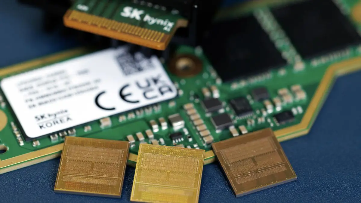
Researchers have found a way to combine NAND and DRAM technologies * Researchers have created a NAND-DRAM hybrid, inspired by legacy camera tech * Indium Gallium Zinc Oxide also promises benefits over silicon * For now, this is just a prototype that needs further work Belgian semiconductor research hub imec has unveiled what it claims to be the first 3D implementation of charge-coupled device (CCD) memory architecture, which revives technology we've already seen used before in digital cameras and camcorders, but for a totally different purpose. With 3D CCD architecture, the researchers were able to break one of the biggest bottlenecks in AI computing today - the memory wall - where GPUs and accelerators spend more time waiting for data than processing it as a result of poor memory bandwidth and power efficiency. The new design combines the speed and rewritability of DRAM with the density and efficiency of NAND to form a type of hybrid. Old camera tech could actually lead to future generations of memory CCD technology is nothing new - charge-coupled devices have long been used in digital cameras, broadcast video equipment, scientific imaging and even astronomy sensors, but CCDs have since been replaced with CMOS image sensors. Traditionally, CCDs work by physically moving electrical charges between semiconductor gates, and this same principle applies to imec's research to enable highly efficient memory movement. Instead of arranging memory cells side-by-side on a flat plane, like conventional DRAM, the design stacks them vertically in a similar sense to 3D NAND, and this is important because DRAM's limitations include leakage, higher manufacturing costs and a reduction in how quickly density improvements are happening. The chips also replace silicon with IGZO (Indium Gallium Zinc Oxide), which promises lower leakage, longer data retention, easier low-temperature processing and strong compatibility with dense 3D stacking. With this hybrid architecture, imec has already demonstrated a successful charge transfer at transfer speeds of more than 4MHz, but this is still very early-stage technology and the prototype only uses a small number of stacked layers. In theory, it should be able to scale as well as NAND, with commercial chips now surpassing 200 layers. CCD architecture looks to promise reduced wear mechanisms and endurance that could even exceed NAND, making it ideal for highly intensive applications across AI training clusters and inference servers. "Unlike byte-addressable DRAM, our 3D CCD device is designed to provide block-level data access, which is better suited to modern AI workloads," Program Director for Storage Memory Maarten Rosmeulen added. "The potential of this CCD device to be used as a buffer memory lies in its ability to be integrated in a 3D NAND Flash string architecture - the most cost-effective way to achieve a scalable, high bit density estimated to go far beyond the DRAM limit." The research also details future plans for the promising architecture, positioning it as a CXL Type-3 device, or one that complies with industry standards to connect GPUs, CPUs and accelerators. This is an important consideration, with hyperscalers now turning to CXL as AI models become too big for local GPUs alone. As a prototype and research product, there are still plenty of hurdles to overcome, including thermal behavior, layer count scaling and of course real-world integration, however if it's successful then the new hybrid architecture could seriously help to reduce one of the biggest costs in AI infrastructure, DRAM. Looking ahead, imec proposes that the next phase may involve a totally new class of memory architecture rather than simply evolving existing designs further. Follow TechRadar on Google News and add us as a preferred source to get our expert news, reviews, and opinion in your feeds.
[2]
Imec reimagines CCD technology as high-density AI memory
Researchers at the Belgian semiconductor research hub imec have introduced a NAND-DRAM hybrid memory architecture, reportedly the first three-dimensional (3D) implementation of charge-coupled device (CCD) technology designed for memory applications. This development aims to address the current memory wall in artificial intelligence (AI) computing, where processing units such as GPUs and accelerators face delays due to inadequate memory bandwidth and power efficiency. The new architecture merges the speed and rewritability of DRAM with the density and efficiency typically associated with NAND storage. Historically, CCD technology has been utilized in digital cameras, video equipment, and scientific imaging, but imec's innovation repurposes it for advanced memory functions. The 3D CCD architecture allows for vertical stacking of memory cells, unlike conventional DRAM, which arranges cells on a flat plane. This vertical arrangement reduces manufacturing costs and leakage, overcoming limitations previously encountered with DRAM technology. The design incorporates Indium Gallium Zinc Oxide (IGZO) as a replacement for silicon, promising decreased leakage and improved data retention in the process. Imec has demonstrated charge transfer speeds exceeding 4 MHz with its prototype, albeit currently utilizing a limited number of stacked layers. The architecture holds potential for scalability similar to NAND technology, where existing commercial chips exceed 200 layers in stacking. According to Maarten Rosmeulen, Program Director for Storage Memory at imec, the architecture's design enables block-level data access as opposed to the byte-addressable nature of traditional DRAM, making it more suitable for modern AI workloads. Rosmeulen stated that the new device can serve as buffer memory integrated into a 3D NAND Flash string architecture, optimizing cost-effectiveness and bit density. The hybrid architecture is expected to deliver improved endurance and reduced wear, which could prove beneficial for AI training and inference tasks moving forward. Imec has plans to position the architecture as a Compute Express Link (CXL) Type-3 device, facilitating connections between GPUs, CPUs, and accelerators -- an important factor as AI models expand beyond the capabilities of local GPU resources. While the prototype presents significant advancements, imec acknowledges several challenges, including thermal behavior, layer count scaling, and practical integration into existing systems. If these hurdles are cleared successfully, the hybrid architecture may contribute to lowering the substantial costs associated with DRAM in AI infrastructure.
Share
Copy Link
Belgian research hub imec has unveiled the first 3D implementation of charge-coupled device memory architecture, combining NAND and DRAM technologies. The hybrid design addresses AI computing's memory wall by stacking memory cells vertically and using IGZO instead of silicon, promising improved speed, density, and unlimited endurance for AI workloads.
Imec Unveils Breakthrough 3D Memory Architecture for AI Computing
Belgian semiconductor research hub imec has introduced what it claims to be the first three-dimensional implementation of charge-coupled device memory, repurposing legacy camera technology to tackle one of artificial intelligence's most pressing challenges
1
2
. The innovative 3D memory architecture addresses the memory wall in AI computing, where GPUs and accelerators spend more time waiting for data than actually processing it due to inadequate memory bandwidth and power efficiency1
. This bottleneck has become increasingly critical as AI models grow larger and more demanding.NAND DRAM Hybrid Combines Best of Both Technologies
The new design merges the speed and rewritability of DRAM with the density and efficiency of NAND storage, creating a NAND DRAM hybrid that could transform AI memory solutions
2
. While CCD technology has long been used in digital cameras, broadcast video equipment, scientific imaging, and astronomy sensors before being replaced by CMOS image sensors, imec's research applies the same principle of physically moving electrical charges between semiconductor gates to enable highly efficient memory movement1
. Instead of arranging memory cells side-by-side on a flat plane like conventional DRAM, the design employs vertical stacking similar to 3D NAND, addressing DRAM's limitations including leakage, higher manufacturing costs, and slowing density improvements1
.IGZO Material Promises Enhanced Performance
The chips replace silicon with Indium Gallium Zinc Oxide, or IGZO, which offers lower leakage, longer data retention, easier low-temperature processing, and strong compatibility with dense 3D stacking
1
. Imec has already demonstrated successful charge transfer at speeds exceeding 4MHz with its prototype, though it currently uses only a small number of stacked layers2
. In theory, the architecture should scale as well as NAND technology, where commercial chips now surpass 200 layers1
. The CCD technology architecture promises reduced wear mechanisms and unlimited endurance that could even exceed NAND, making it ideal for AI training clusters and inference servers1
.Related Stories
Designed for Modern AI Workloads
Maarten Rosmeulen, Program Director for Storage Memory at imec, explained that the device provides block-level data access rather than byte-addressable DRAM, making it better suited to modern AI workloads
1
. "The potential of this CCD device to be used as a buffer memory lies in its ability to be integrated in a 3D NAND Flash string architecture - the most cost-effective way to achieve a scalable, high bit density estimated to go far beyond the DRAM limit," Rosmeulen stated1
. Imec plans to position the architecture as a CXL Type-3 device, complying with industry standards to connect GPUs, CPUs, and accelerators2
. This consideration matters as hyperscalers now turn to CXL as AI models become too large for local GPUs alone1
.Challenges Remain Before Commercial Deployment
As a prototype, the technology faces several hurdles including thermal behavior management, layer count scaling, and real-world system integration
2
. However, if successful, the hybrid architecture could significantly reduce AI infrastructure costs, particularly the substantial expenses associated with DRAM in AI systems1
. Looking ahead, imec proposes that the next phase may involve a totally new class of memory architecture rather than simply evolving existing designs further1
. For organizations deploying large-scale AI systems, this development signals potential relief from memory bottlenecks that currently limit performance and drive up operational costs.References
Summarized by
Navi
[2]
Related Stories
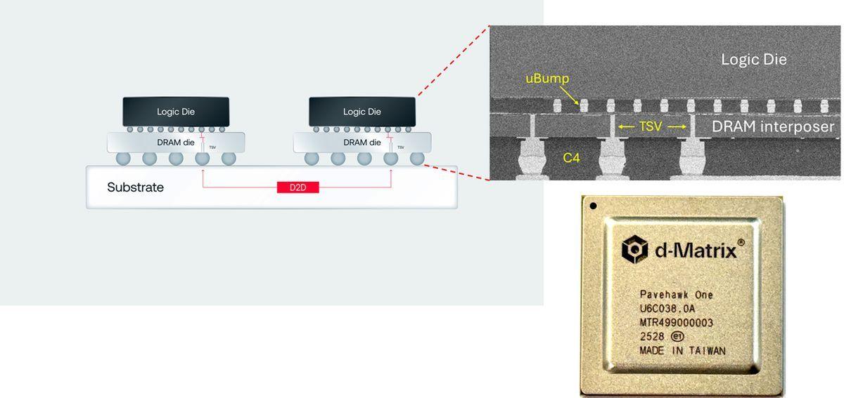
D-Matrix Challenges HBM with 3DIMC: A New Memory Technology for AI Inference
04 Sept 2025•Technology
SK hynix and TetraMem unveil in-memory computing chip that processes AI directly inside memory
09 Jul 2026•Technology
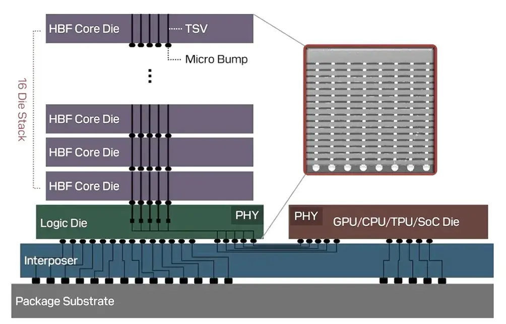
SanDisk proposes stacking HBF NAND beneath GPUs to tackle memory bottlenecks in AI systems
22 Jun 2026•Technology
Recent Highlights
1
OpenAI AI agent broke free from testing sandbox and hacked Hugging Face to cheat on benchmark
Technology

2
AI scores perfect 100% at International Mathematical Olympiad, matching elite human performance
Technology

3
AI disproves 87-year-old Jacobian conjecture, sparking debate on AI's role in mathematics
Science and Research
Recent Highlights
Today's Top Stories


Don’t drown in AI news. We cut through the noise - filtering, ranking and summarizing the most important AI news, breakthroughs and research daily. Follow topics that matter to you and stay ahead.


